Skip to content

From wafer development to final testing, each layer of your semiconductor device relies on precision and control. Vitrek delivers advanced test and measurement solutions that enable you to monitor, verify, and optimize every stage of the process—without slowing production or sacrificing quality. Our scalable platforms support metrology, displacement sensing, and electrical safety testing, helping manufacturers produce superior semiconductors—one flawless layer at a time. Here are some examples of our capabilities.
Wafer Metrology
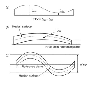
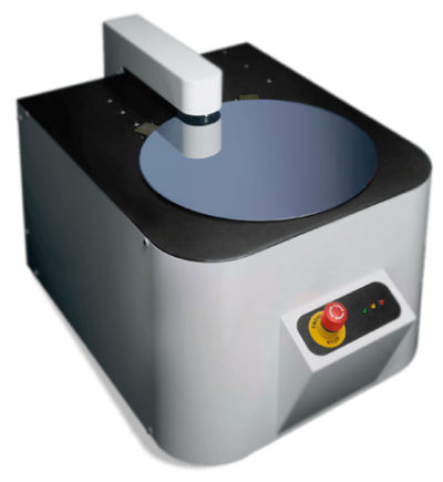
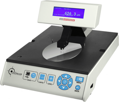
- Monitoring wafers during preparation stages to check thickness for compliance with minimal bow, warp, and total thickness variation (TTV).
- In-process monitoring of solar/photovoltaic wafers for multi-channel thickness, TTV, and bow measurement.
- Ultrasonic, non-destructive inspection of wafers for potential flaws or manufacturing defects.
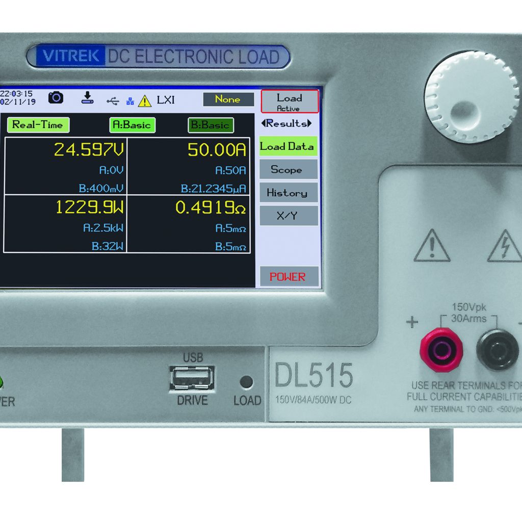
Test & Characterization
- Operational testing and characterization of packaged semiconductor devices.
- Software utilized in high-speed PASS/FAIL testing systems.
- Signal simulation for calibrating data acquisition systems and providing precision voltages for device testing.
- Real-time acquisition and analysis of storage media read-and-write head signals in manufacturing.
- Real-time ultrasonic characterization of semiconductor die adhesion in manufacturing.
Fabrication Capital Equipment
- Sensors used in the high-resolution focusing of complex lens systems in photolithography tools.
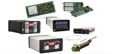
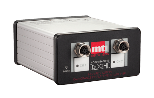
- Sensors utilized to deliver precise measurements of displacement, active vibration, position, and distance.
- Digitizers used in real-time process control for characterization of fabrication processes, enabling fast device control loops with short data latency.
- Design and production testing in a wide range of fabrication gear.
Applications
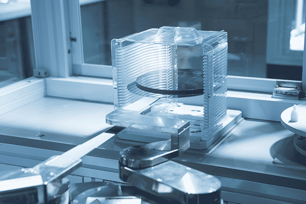
Wafer QA/QC after Slicing and Polishing
Sensors utilized to deliver precise measurements of displacement, active vibration, position, and distance.
Application NoteWafer Measurement – Ungrounded
Sensors utilized to deliver precise measurements of displacement, active vibration, position, and distance.
Application NoteWafer Bow And Warp Measurement Systems
Sensors utilized to deliver precise measurements of displacement, active vibration, position, and distance.
Application NoteCapacitance Sensors Facilitate 3D IC Construction
Sensors utilized to deliver precise measurements of displacement, active vibration, position, and distance.
Application NotePush-Pull Capacitance Sensor Measures Ungrounded Targets
Sensors utilized to deliver precise measurements of displacement, active vibration, position, and distance.
Application NoteProducts
>


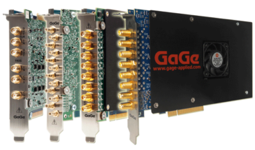
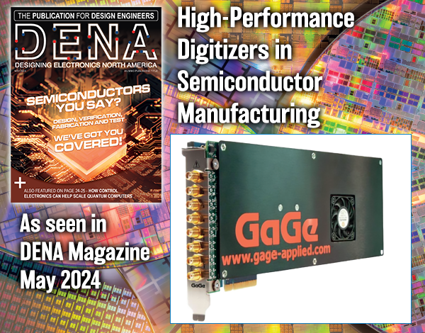
High-Speed Digitizers
GaGe high-speed digitizers provide ultra-fast sampling, deep memory, and low-latency processing for precise semiconductor testing and process monitoring.


Videos