 Skip to content
Blogs
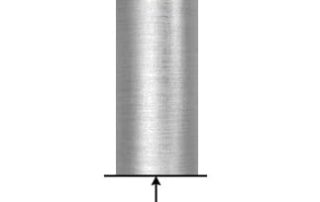
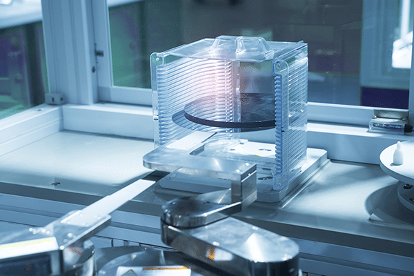
LED SUBSTRATE THICKNESS
Industry Semiconductor Applications Photolithography Using Capacitance Sensors Measurement Type Positioning Description Remember that old acronym, GIGO? Garbage in garbage out, it can apply to raw materials as well as programming. Sapphire wafers need to be of a certain quality to ensure maximum yield. Excessive TTV, Bow, and Warp lead to premature LED failure. LED manufacturers need to inspect incoming wafers. Wafer producers also need to check and control TTV, Bow and Warp. The market for sapphire wafers, driven by the growth in LED manufacturing, is booming. While the price [...]
Sales Network
Sales Network United States Choose the pin closest to your location to contact your Vitrek Regional Manager. International Europe Choose the pin closest to your location to view Vitrek partners in your area. Asia Choose the pin closest to your location to view Vitrek partners in your area. South America Choose the pin closest to your location to view Vitrek partners in your area. [...]
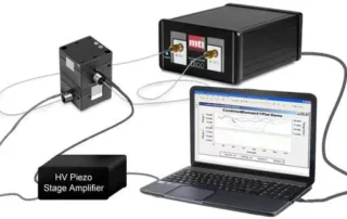
PIEZO STAGE POSITIONING
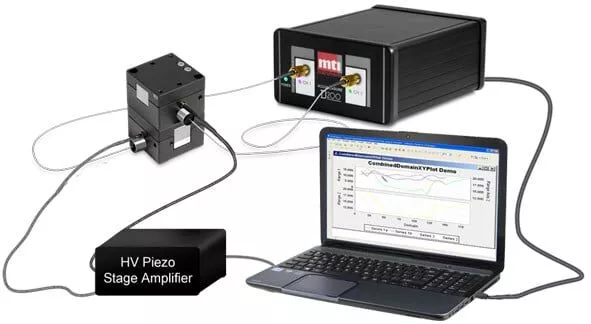
Industry Consumer Electronics Applications Piezo Stage Measurement Type Positioning Description Positioning stages using piezoelectric stack actuators (PEA) have very high resolution. However, it is difficult to achieve precise dynamic motion tracking using traditional linear controllers such as PID due to the inherent hysteresis nonlinearity of piezoelectric materials and the phase lag associated with such controllers. Capacitance Sensors are ideal for measuring the actual piezo stage position and correcting for the inherent nonlinearity through closed loop feedback. They have the stability, bandwidth and high resolution needed to do the job. [...]

WAFER QA/QC AFTER SLICING AND POLISHING
Industry Semiconductor Applications Wafer Qa/Qc After Slicing And Polishing Measurement Type Surface Description When wafers are sliced up with wire saws, they are measured to make sure they are within the specified thickness, with minimal bow, warp, and TTV. After initial measurement, they are sorted and sent for polishing. Since polishing removes material and smoothes out the rough surfaces they need to be measured again to ensure they meet thickness guidelines and quality standards. Solution: MTI Instruments manufactures multiple systems to perform thickness measurements. From semi automated Proforma 300SA to manual wafer [...]
ABOUT WAFER BOW AND WARP MEASUREMENT SYSTEMS
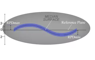
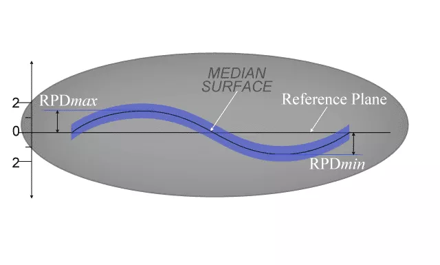
Thickness Measurement for Metrology Systems ASTM F657: The distance through a wafer between corresponding points on the front and back surface. Thickness is expressed in microns or mils (thousandths of an inch). Total Thickness Variation (TTV) ASTM F657: The difference between the maximum and minimum values of thickness encountered during a scan pattern or series of point measurements. TTV is expressed in microns or mils (thousandths of an inch). ASTM F534 3.1.2: The deviation of the center point of the median surface of a free, unclamped wafer from the median [...]
LITHOGRAPHY OPTICS POSITION FOCUS
Industry Semiconductor Applications Photolithography Using Capacitance Sensors Measurement Type Positioning Description One specific area where capacitance systems excel is high resolution focusing of complex lens systems such as those found in atomic force microscopes, vision inspection machines and photolithography tools. In a multi-million dollar photolithography tool, high accuracy, nanometer resolution and maximum thermal stability are absolutely critical to maintain proper focus and obtain integrated circuit line widths as small as 45 nanometers. Additionally, most systems demand low power consumption and maximum heat dissipation to eliminate any adverse affects from [...]

GAAS SUBSTRATE THICKNESS MEASUREMENT
Industry Semiconductor Applications Gaas Substrate Thickness Measurement Measurement Type Thickness Description Measuring Thickness of Wafers with Different Chemistries Introduction: Silicon wafers are ordinarily highly conductive and easy to measure with standard capacitive displacement sensors (See MTI’s Proforma 300i). Measuring the thickness of GaAs wafers that have high bulk resistivity (>10k Ohm/cm) is a little more difficult because the wafers act as non-conductive insulators in a capacitive sensor’s measuring field. Fortunately, MTI has a solution to this problem. Solution: It’s possible to measure the thickness and TTV of high resistivity semiconducting wafers (like GaAs) using non-contact capacitive [...]
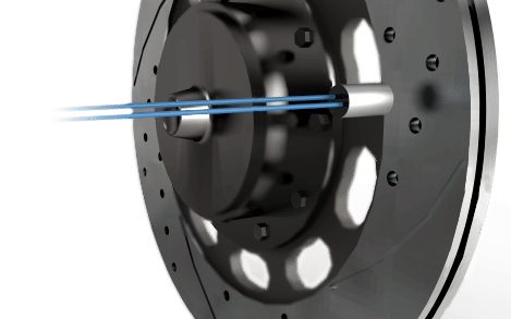
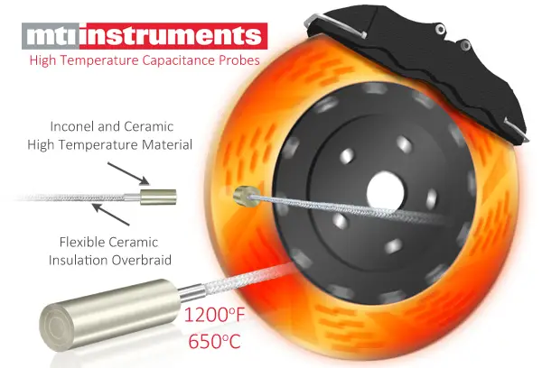
SPINDLE RUN OUT
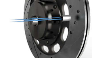
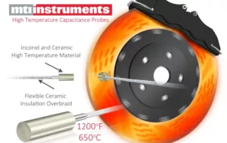
Industry Automotive Applications Spindle Run Out Measurement Type Positioning Description Rotating targets frequently have an intermittent, uncertain or nonexistent ground path. This introduces unwanted noise, instability, drift and reduces accuracy of the measurement. MTI Instruments offers a unique “Push-Pull” capacitance measurement system that does not require a grounded target. It utilizes two probes, built into one body, that work together to complete the ground path. One probe pushes current into the brake rotor while the adjacent probe pulls the current out. The result is a “clean”, consistent electrical sensing path. As [...]

Windshield Manufacturing
Industry Automotive Applications Oil Film Measurement Type Level Description In order to maintain proper profile and thickness within a glass furnace the extrusion plate spacing must be maintained at a predetermined gap. Unfortunately, due to process changes and temperature swings this gap can fluctuate significantly in short periods of time. This variation causes the glass thickness to change (check out our glass thickness measurement devices to accurately measure thickness), producing uneven temperature gradients and creating potentially weak glass panels. To control this critical parameter the manufacturing process requires automated active feedback [...]
BRAKE ROTORS THICKNESS VARIATION
Industry Automotive Applications Brake Rotors Thickness Variation Measurement Type Surface Description Driving cross country or cross town, we give little thought to the operation or complexity of our vehicle braking systems. They only cross our mind when we absolutely need them; we never stop to think about the extensive design and testing that makes them such a lifesaver. Take the brake rotor for example. Under normal operating conditions it’s subjected to extreme temperatures and forces, which can cause rotor distortion and potential failure. To make certain it can withstand [...]