 Skip to content
Blogs
 Capacitance Sensing Provides Two Ways to Measure EV Battery Plate Thickness Gallery
Capacitance Sensing Provides Two Ways to Measure EV Battery Plate Thickness
Application Notes-MTI, Brand-MTI, Industry-Automotive, Industry-Energy, Industry-Manufacturing, News-MTI, News-MTI-Instrumentation, News-MTI-Metrology, News-Product Updates, Products-MTI-Capacitance, Products-MTI-Laser/Fiber Optic, Products-MTI-Semiconductor/Metrology, Z-REPUB, z1
Capacitance Sensing Provides Two Ways to Measure EV Battery Plate Thickness
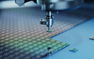
MTI Instruments has released an application note that explains how to use capacitance to measure the thickness of the lithium battery plates in electric vehicles (EVs). Manufacturers need to check these plates for thickness before calendaring them together to ensure that the overall battery diameter is within specifications. In EV batteries, lithium ion compounds are applied to either a copper plate substrate (cathode) or an aluminum substrate (anode plate). These conductive plates are separated by a dielectric. MTI Instruments, a global supplier of precision measurement solutions, makes capacitance sensors that can measure thicknesses materials down to nanometers. Moreover, MTI [...]
 Trends in High Resolution Sensors for Semiconductor Metrology and Inspection Gallery
Trends in High Resolution Sensors for Semiconductor Metrology and Inspection
Application Notes-MTI, Brand-MTI, Industry-Compliance Testing, Industry-Consumer Products, Industry-Electronics, Industry-Manufacturing, Industry-Semiconductor, Industry-Semiconductor-MTI, Products-MTI-Capacitance, Products-MTI-Semiconductor/Metrology, Z-REPUB, z1
Trends in High Resolution Sensors for Semiconductor Metrology and Inspection
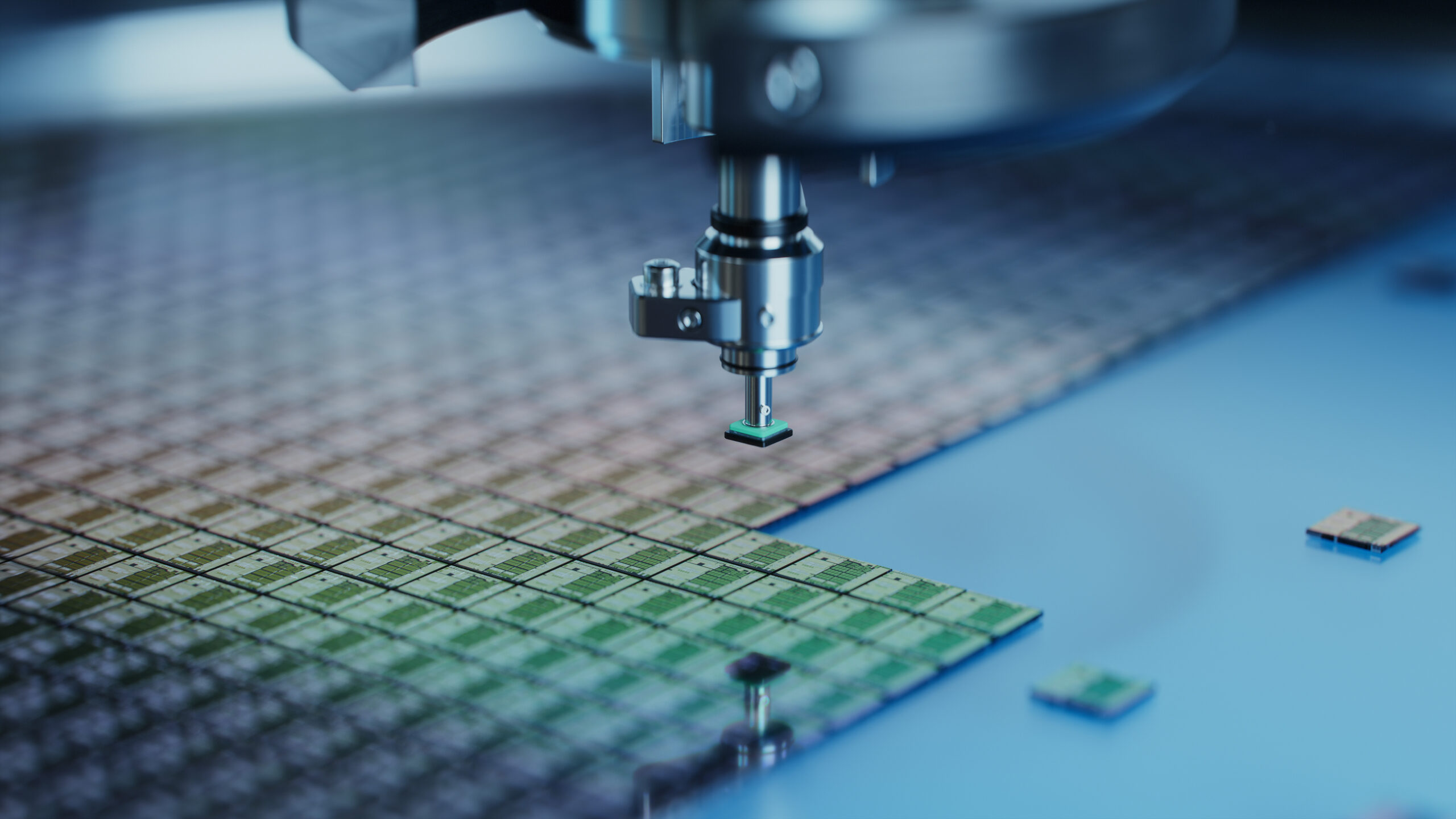
High resolution sensors are supporting improvements in semiconductor metrology and inspection at vital points in the production process. Because the fabrication of semiconductor wafers may require hundreds of steps and weeks of manufacturing time, early-stage defects that go undetected can have costly downstream consequences. Plus, because semiconductor processing always requires a high degree of precision, advances in fabrication methods seem to require ever-finer measurements in a never-ending quest. Today’s metrology instruments are incorporating high resolution sensors for automated wafer inspection. Resolution, the smallest measurement that a sensor can reliably indicate, may be given in dimensional units such as nanometers [...]
 Proforma 300i SA Video Shows Semiconductor Metrology Gallery
Proforma 300i SA Video Shows Semiconductor Metrology
Brand-MTI, Industry-Compliance Testing, Industry-Consumer Products, Industry-Electronics, Industry-Manufacturing, Industry-R&D, Industry-Semiconductor, Industry-Semiconductor-MTI, News-MTI-Metrology, News-Product Updates, Press Releases-Vitrek, Products-MTI-Semiconductor/Metrology, Videos-MTI, Videos-MTI-Manual Semiconductor Metrology System, Z-REPUB, z1
Proforma 300i SA Video Shows Semiconductor Metrology
MTI Instruments, a worldwide leader in precision measurement solutions, has released a YouTube video that shows how its Proforma™ 300i SA semi-automated measurement tool measures silicon carbide wafers for semiconductors. George Relan, MTI’s Global Director of Sales, demonstrates how the desktop metrology system provides non-contact full wafer scanning and 3D mapping of measurement features such as thickness and shape. MTI’s video also shows how the Proforma 300i SA interfaces with an external computer and provides powerful Windows-based software for analysis and reporting. By utilizing MTI push/pull technology, the Proforma 300i SA doesn’t require the semiconductor wafers to have a [...]
Measurement Applications
Measurement Applications Application Notes by Measurement Type Whatever our customers are trying to measure precisely, MTI Instruments has a tool. From getting accurate distances and thicknesses to precise vibration analysis, our measurement systems and tools are used by industry leaders around the world. Take a look at the measurement types below to see the variety of tools we have for various applications that help our customers.
Manual Semiconductor Metrology System
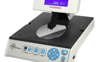
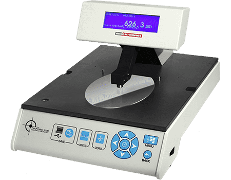
Cost-effective alternative to full-automated wafer measurement and inspection systems Request a Quote Download Brochure Product can provide measurement of thickness and bow of all wafer materials including Silicon, Gallium-Arsenide, Indium-Phosphide and sapphire or tape. The Proforma 300i wafer thickness gauge is a capacitance based, differential measurement system that performs non-contact thickness measurements of semiconducting and semi-insulating wafers. By utilizing MTI Push/Pull technology, the Proforma 300i does not require the wafers to have a consistent electrical ground resulting in exceptional accuracy and repeatability for most wafer types. The Proforma 300i system includes full remote control operating software [...]
Download How to Reduce Inconsistent Wafer Measurements
Thank you for downloading! Here's the link to How to Reduce Inconsistent Wafer Measurements.
Increase SiC Wafer Production Yield
Demand for SiC wafers is growing rapidly and production needs to keep up. Speeding up production can result in higher defect rates without the proper inspection equipment in place during the R&D process, where poor verification of your process tools can dramatically reduce yield. MTI Instruments 300iSA system can help measure TTV, flatness, bow and warp of up to 20 wafers per hour. Our solution helps you perform wafer inspection verifications at scale and increases the throughput of your production yield as the demand grows for 100-200mm diameter wafers. Finding defects at volume can be difficult, but MTI’s superior [...]
Target Material and Characteristics
Target Material and Characteristics Transparent/Opaque Targets There are a number of measurement systems that are capable of measuring a target that is opaque. When it comes to transparent targets, the measurement system being used must match the material of the target being measured. For example, if you’re attempting to measure plastic you should use a contact-type measurement system such as a micrometer. When performing a soft target measurement, such as film, a non-contact measurement system (such as a laser displacement sensor) should be utilized. Hard/Soft Targets Objects made out of hard material (such as a block of wood), would [...]
Semiconductor/Solar Metrology Systems
Semiconductor/Solar Metrology Systems Manual Semiconductor Metrology System The Proforma 300i wafer thickness gauge is a capacitance-based, differential measurement system that performs non-contact thickness measurements of semiconducting and semi-insulating wafers. View Product Semi-automated Metrology System The Proforma 300iSA is a benchtop/desktop, semi-automated wafer measurement system for semi-conducting and semi-insulating materials delivering full wafer surface scanning for thickness, thickness variation, bow, warp, sori, site and global flatness. View Product WAFER MEASUREMENT TOOL One of the most important components of your electrical devices is the semiconductor wafers that [...]