 Skip to content
Blogs
 Why Disc Geometry Matters In Wafer Production Gallery
Why Disc Geometry Matters In Wafer Production
Application Notes-MTI, Brand-MTI, Industry-Consumer Products, Industry-Electronics, Industry-Manufacturing, Industry-Semiconductor, Industry-Semiconductor-MTI, News-MTI-Metrology, Products-MTI-Semiconductor/Metrology, z1
Why Disc Geometry Matters In Wafer Production
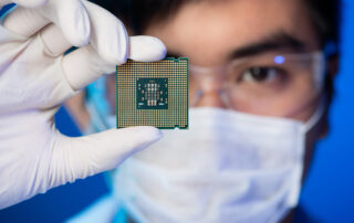
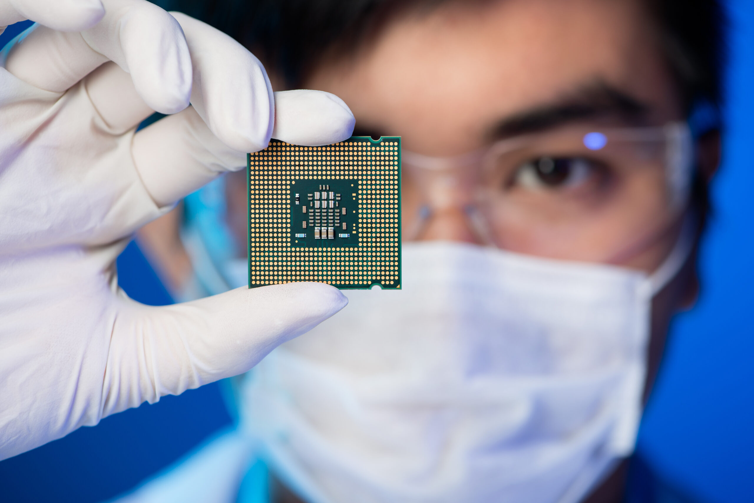
This is the first of three articles in Semiconductor Wafer Measurement for Increased Profitability. The second article examines the cost of failing to inspect semiconductor wafers. The third article describes the benefits of using semi-automated, fully-automated, and manual systems for wafer metrology and inspection. Semiconductor wafers are cut from cylindrical silicon crystals, or ingots. The flatness of these disc-shaped wafers is controlled to tight tolerances to ensure that the entire wafer surface is suitable for integrated circuit (IC) production. If disc geometry is out-of-spec after cutting, it may be possible to reprocess the wafer. Cutting is only the first [...]
 Advantages of Measuring Semiconductor Thin Film Thickness with Capacitance Gallery
Advantages of Measuring Semiconductor Thin Film Thickness with Capacitance
Application Notes-MTI, Brand-MTI, Industry-Compliance Testing, Industry-Electronics, Industry-Manufacturing, Industry-R&D, Industry-Semiconductor, Industry-Semiconductor-MTI, Industry-Sensors, Products-MTI-Capacitance, Products-MTI-Laser/Fiber Optic, Products-MTI-Semiconductor/Metrology, Z-REPUB, z1
Advantages of Measuring Semiconductor Thin Film Thickness with Capacitance
Semiconductor Thin Films: Measuring Thickness with Capacitance In the semiconductor industry, thin films are deposited onto silicon and other wafer materials one atomic layer at a time. The thickness of these extremely thin coatings is important because thin-film thickness affects the wafer’s electrical, optical, and mechanical properties. With semiconductors, either conductive metallic films or non-conductive metal oxide films are deposited. There are two main thin-film coating methods, chemical vapor deposition (CVD) and physical vapor deposition (PVD), both of which use a variety of processes. Because the coatings for semiconductor wafers are so thin, thickness measurement require a high degree [...]
 Why Demand for SiC Wafers is Hot and Durable Gallery
Why Demand for SiC Wafers is Hot and Durable
Brand-MTI, Industry-Consumer Products, Industry-Electronics, Industry-Manufacturing, Industry-Semiconductor, Industry-Semiconductor-MTI, MTI Blog, News-MTI, News-MTI-Metrology, Products-MTI-Semiconductor/Metrology, Z-REPUB, z1
Why Demand for SiC Wafers is Hot and Durable
Why Demand for SiC Wafers is Hot and Durable Pardon the pun, but SiC wafers are a hot item for high-temperature applications. Silicone carbide (SiC), a semiconductor containing both silicon and carbide, withstands temperatures up to 2700°C. Carborundum, as this durable ceramic is also known, finds additional applications in bulletproof vests, extrusion dies, sandpaper, and high-performance disc brakes. In electronics, SiC materials are used with light-emitting diodes (LEDs) and detectors. In the semiconductor industry, a market where interest is red-hot, SiC wafers are used in electronic devices that operate at high temperatures, high voltages, or both. Examples include electric [...]
Wafer Stress Analysis Using the 300iSA
Wafer Stress Analysis Using MTI Instruments Proforma 300iSAWafer processing involves several stages that may translate into mechanical alterations. Sometimes these alterations can cause deformities that render the wafer either unusable or that put it marginally close to not being usable. To determine this, stress analysis can be used.The Proforma 300iSA wafer characterization tool provides a software capability in which a wafer can be analyzed prior to processing and then after processing. The tool then evaluates how the wafer changed and hence, provides the resulting stress analysis.The software expects the customer to provide the material elasticity constants and to define them [...]
 CMP and Capacitance-Based Semiconductor Wafer Measurement Gallery
CMP and Capacitance-Based Semiconductor Wafer Measurement
Application Notes-MTI, Brand-MTI, Industry-Compliance Testing, Industry-Consumer Products, Industry-Electronics, Industry-Manufacturing, Industry-Semiconductor, Industry-Semiconductor-MTI, Industry-Sensors, Products-MTI-Capacitance, Products-MTI-Semiconductor/Metrology, z1
CMP and Capacitance-Based Semiconductor Wafer Measurement
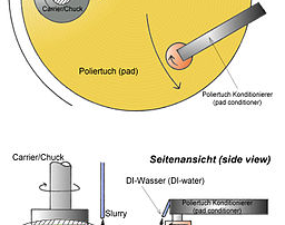
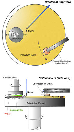
Chemical mechanical polishing (CMP) uses chemical oxidation and mechanical abrasion to selectively remove material from semiconductor wafers in order to achieve very high levels of planarity. The planarity, or flatness, of these wafers is important for optical lithography, a microfabrication technique that produces integrated circuits (ICs) by transferring a geometric pattern from a photomask to a light-sensitive chemical photoresist. Also known as photolithography or UV lithography, optical lithography can produce a geometric pattern on a thin film or directly onto the substrate. Semiconductor Wafer Measurements: Flatness and Shape During optical lithography, variations in wafer flatness must be smaller than [...]
 MEMS and Capacitance-Based Semiconductor Wafer Measurement Gallery
MEMS and Capacitance-Based Semiconductor Wafer Measurement
Application Notes-MTI, Brand-MTI, Industry-Compliance Testing, Industry-Consumer Products, Industry-Electronics, Industry-Manufacturing, Industry-Semiconductor, Industry-Semiconductor-MTI, Industry-Sensors, Products-MTI-Capacitance, Products-MTI-Semiconductor/Metrology, Z-REPUB, z1
MEMS and Capacitance-Based Semiconductor Wafer Measurement
MEMS Technology and Capacitance-Based Wafer Measurement Micro-electrical-mechanical systems (MEMS) are tiny devices that house electrical and mechanical components on a single silicon chip or integrated circuit (IC). They integrate mechanical structures with electronics that are normally fabricated with complementary metal-oxide-semiconductor (CMOS) technologies. In addition to miniaturization, the benefits of MEMS include expanded functionalities at lower cost and with improved performance and reliability. With MEMS devices, critical physical dimensions range from smaller than one micron (µ) to larger than several millimeters (mm). In complex systems, multiple moving elements may be controlled by integrated electronics. Examples of the mechanical components in [...]
 Wafer Backgrinding and Semiconductor Thickness Measurements Gallery
Wafer Backgrinding and Semiconductor Thickness Measurements
Application Notes-MTI, Brand-MTI, Industry-Compliance Testing, Industry-Consumer Products, Industry-Electronics, Industry-Manufacturing, Industry-Semiconductor, Industry-Semiconductor-MTI, News-MTI-Instrumentation, News-MTI-Metrology, Products-MTI-Capacitance, Products-MTI-Semiconductor/Metrology, Z-REPUB, z1
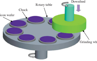
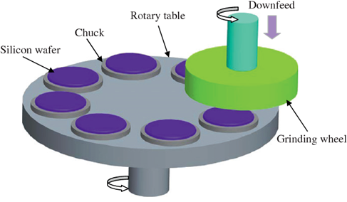
Wafer Backgrinding and Semiconductor Thickness Measurements
Wafer backgrinding is the first step in semiconductor packaging, the process of encasing one or more discrete semiconductor devices or integrated circuits (IC) for protection. Known also as wafer thinning or wafer lapping, backgrinding reduces wafer thickness to allow stacking and high-density IC packaging. Wafer thickness also determines package height, an important consideration as smartphones, laptops, and other electronic devices become thinner. With MEMS, wafer thinning also controls the proof mass for devices such as accelerometers or the diaphragm thickness for pressure sensors. Etching the surface of the wafer produces the IC but grinding the backside is what produces [...]
 Transducer Selection for High Resolution Applications Gallery
Transducer Selection for High Resolution Applications
Application Notes-MTI, Brand-MTI, News-MTI-Instrumentation, News-MTI-Metrology, News-Product Updates, News-Products, Products-MTI-Capacitance, Products-MTI-Laser/Fiber Optic, Products-MTI-Semiconductor/Metrology, Products-MTI-Signal Generators, Z-REPUB, z1
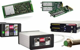
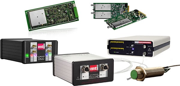
Transducer Selection for High Resolution Applications
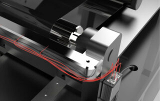
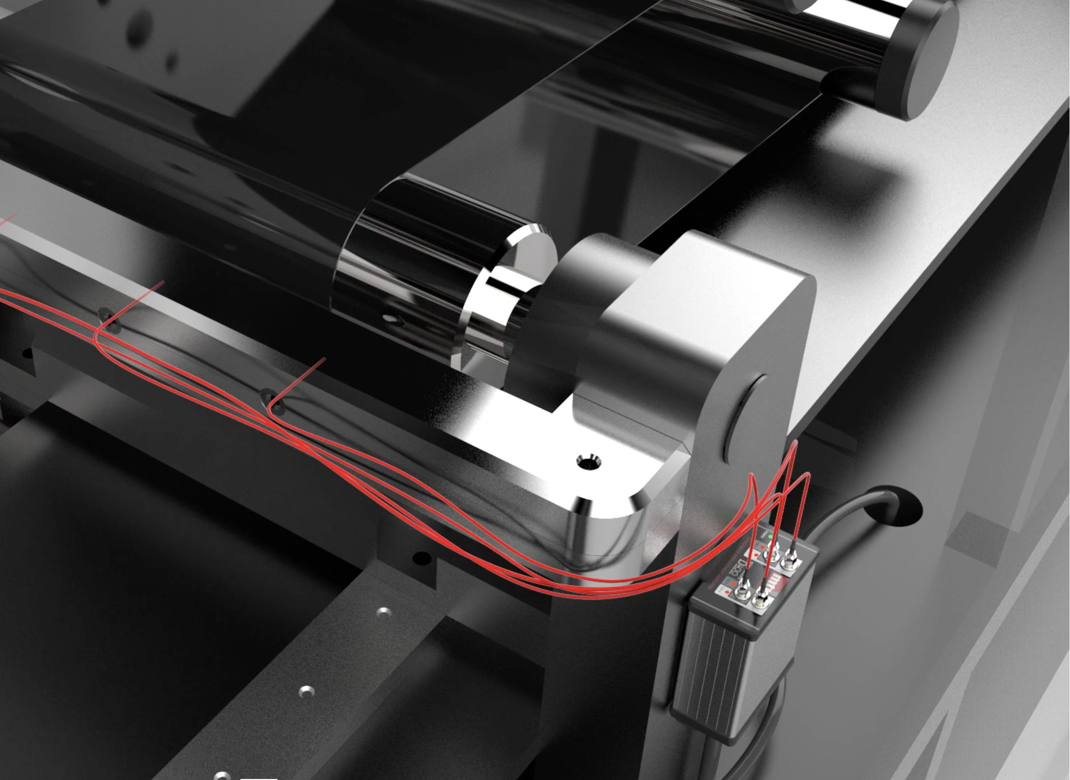
High resolution applications do not always require an interferometer. If you want to make accurate measurements in the micron to picometer range, then an MTI Digital Accumeasure D100 HD or D200 system may be what you need. Laser interferometers can sell for more than $15,000 and be difficult to setup. For example, you may have to buy additional optics to guarantee a good return signal since the laser beam must reflect off a mirror surface or precision retro reflector in order for the beam to re-enter the interferometer’s optics at less than a degree of reflection angle. The downsides [...]
 High Resolution Semiconductor Wafer Measurements at Lower Costs Gallery
High Resolution Semiconductor Wafer Measurements at Lower Costs
Application Notes-MTI, Brand-MTI, Industry-Consumer Products, Industry-Electronics, Industry-Manufacturing, Industry-Semiconductor, Industry-Semiconductor-MTI, Products-MTI-Capacitance, Products-MTI-Semiconductor/Metrology, Z-REPUB, z1
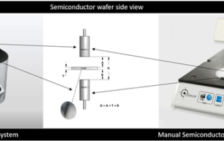
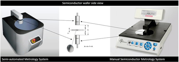
High Resolution Semiconductor Wafer Measurements at Lower Costs
MTI's Proforma technology characterizes semiconductor wafers in terms of bow and warp, thickness, total thickness variation (TTV) and center thickness. Until recently, semiconductor wafer measurements at resolutions less than 100 µm were cost-prohibitive. Moreover, only expensive devices such as interferometers were capable of these measurements. Today, the semiconductor industry can use capacitance gauges instead of laser interferometers to achieve high resolution at fraction of the cost. Much like affordable CCD cameras transformed and expanded the market for video, cost-effective capacitance is disrupting the semiconductor wafer measurement market and creating new opportunities for quality testing and validation. The [...]
Capacitance Sensing for Non-Contact Thickness Measurements of Insulating Materials
Capacitance sensing can be used to make non-contact thickness measurements for most insulating materials. Capacitance sensors are known for their ability to precisely measure the thickness and position of conductive targets, but what’s less known is that these sensors can also measure the thickness of non-conductive materials. Examples include glass, sapphire, and plastics, as well as semi-insulating semiconductor materials such as GaAs and silicon nitride. Analog vs. Digital Technologies MTI Instruments, a global supplier of precision measurement technologies, takes the guesswork out of what used to be a complex measurement for non-conductive materials. MTI's Digital Accumeasure system features a [...]