 Skip to content
Blogs
Capacitance Sensors vs. Eddy Current Sensors Application Note
Capacitance Sensors vs. Eddy Current Sensors Application Note Capacitance sensors and Eddy current sensors are both used for non-contact measurements. Capacitive probes use electric fields to measure the distance from the sensor face to the surface of a target that is typically conductive and grounded. Eddy current probes use an alternating AC current to induce a magnetic field in a conductive target instead. In turn, the induced magnetic field produces a back magnetic field that is proportional to the gap between the probe face and the target. In a recent application note, MTI Instruments examines the differences between capacitance [...]
Foam Density Measurement: Capacitance Sensors vs. Nuclear Gauges
This application note from MTI Instruments compares two technologies for measuring foam density: capacitance sensors and nuclear gauges. It examines the basic operating principles of each technology and explains why capacitance measurement is recommended for in-line measurement during foam manufacturing. Capacitance Sensors Capacitive probes are non-contact devices that use electric fields to measure foam density. In combination with a thickness value, a density measurement may be calculated. These probes consist of a capacitance sensor inside of a protective housing and are part of a larger measurement system that includes amplifiers, cables, and software. With parallel plate capacitance, the capacitance probe [...]
Capacitance Sensing vs. Strain Gauge Sensing Application Note
Capacitance Sensing vs. Strain Gauge Sensing Application Note Capacitance probes that are embedded in piezo flexure stages can provide significantly greater accuracy than strain gauges. Although some minor mounting modifications are required, capacitance probes with picoscale positioning provide higher linearity, greater long-term stability, and better direct measurement. Capacitance sensors cost more, however, and are limited by sensing distance. Therefore, strain gauge sensors remain a good choice for applications where cost is a consideration, sensing distances are larger, and high resolution or high accuracy are required. In a recent application note, MTI Instruments examines the differences between capacitance probes and [...]
 Using Capacitance Sensors for Non-Conductive Material Measurement Gallery
Using Capacitance Sensors for Non-Conductive Material Measurement
Application Notes-MTI, Brand-MTI, Industry-Compliance Testing, Industry-Consumer Products, Industry-Electronics, Industry-Manufacturing, Industry-Sensors, News-MTI, News-MTI-Instrumentation, Products-MTI-Capacitance, Z-REPUB, z1
Using Capacitance Sensors for Non-Conductive Material Measurement
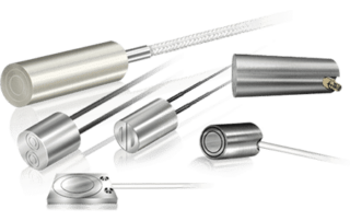
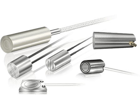
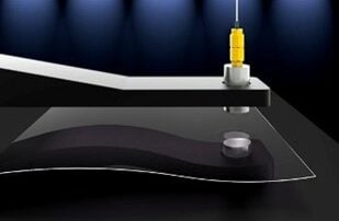
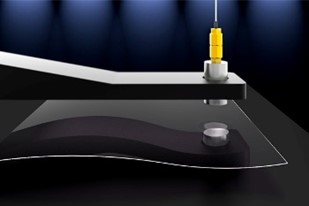
Non-Conductive Material Measurement with Capacitance Sensors Capacitance sensors are non-contact devices that can be used to obtain position, thickness, and dynamic measurements with a high degree of precision, accuracy, and resolution. Capacitive measurement is used with electrically-conductive materials such as metals but can also be used to measure non-conductive materials such as glass, sapphire, and many plastics. Even if a non-conductive material is relatively inexpensive (such as closed cell foam), manufacturers want to avoid errors that can result in significant waste across high volumes. Importantly, capacitance measurement is also used with semi-insulating materials such as gallium arsenide (GaAs) and [...]
 CMP and Capacitance-Based Semiconductor Wafer Measurement Gallery
CMP and Capacitance-Based Semiconductor Wafer Measurement
Application Notes-MTI, Brand-MTI, Industry-Compliance Testing, Industry-Consumer Products, Industry-Electronics, Industry-Manufacturing, Industry-Semiconductor, Industry-Semiconductor-MTI, Industry-Sensors, Products-MTI-Capacitance, Products-MTI-Semiconductor/Metrology, z1
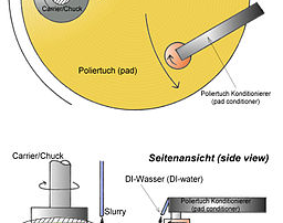
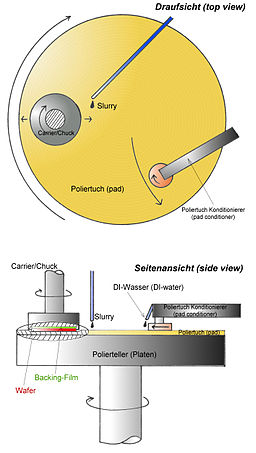
CMP and Capacitance-Based Semiconductor Wafer Measurement
Chemical mechanical polishing (CMP) uses chemical oxidation and mechanical abrasion to selectively remove material from semiconductor wafers in order to achieve very high levels of planarity. The planarity, or flatness, of these wafers is important for optical lithography, a microfabrication technique that produces integrated circuits (ICs) by transferring a geometric pattern from a photomask to a light-sensitive chemical photoresist. Also known as photolithography or UV lithography, optical lithography can produce a geometric pattern on a thin film or directly onto the substrate. Semiconductor Wafer Measurements: Flatness and Shape During optical lithography, variations in wafer flatness must be smaller than [...]
 Multinational Manufacturer Saint-Gobain Selects MTI Instruments’ Digital Capacitance Measurement Technology to Streamline R&D Gallery
Multinational Manufacturer Saint-Gobain Selects MTI Instruments’ Digital Capacitance Measurement Technology to Streamline R&D
Brand-MTI, Industry-Manufacturing, Industry-R&D, News-MTI-Instrumentation, Press Releases-Vitrek, Products-MTI-Capacitance, Z-REPUB, z1
Multinational Manufacturer Saint-Gobain Selects MTI Instruments’ Digital Capacitance Measurement Technology to Streamline R&D
Multinational Manufacturer Saint-Gobain Selects MTI Instruments’ Digital Capacitance Measurement Technology to Streamline R&D ALBANY, N.Y., April 21, 2021 /PRNewswire/ — MTI Instruments, Inc. (“MTI Instruments”), a wholly-owned subsidiary of Mechanical Technology, Incorporated (NASDAQ: MKTY), announced today that Compagnie de Saint-Gobain (“Saint-Gobain”) has selected MTI Instruments’ non-destructive measurement technology to help streamline the Saint-Gobain’s manufacturing research and development. Saint-Gobain, a French multinational corporation that designs, manufactures, and distributes various high-performance materials, chose MTI Instruments as a partner after identifying that the process for producing accurate and repeatable measurement solutions was time-consuming and cost-prohibitive. Saint-Gobain estimated that just 30% of their process [...]
 MEMS and Capacitance-Based Semiconductor Wafer Measurement Gallery
MEMS and Capacitance-Based Semiconductor Wafer Measurement
Application Notes-MTI, Brand-MTI, Industry-Compliance Testing, Industry-Consumer Products, Industry-Electronics, Industry-Manufacturing, Industry-Semiconductor, Industry-Semiconductor-MTI, Industry-Sensors, Products-MTI-Capacitance, Products-MTI-Semiconductor/Metrology, Z-REPUB, z1
MEMS and Capacitance-Based Semiconductor Wafer Measurement
MEMS Technology and Capacitance-Based Wafer Measurement Micro-electrical-mechanical systems (MEMS) are tiny devices that house electrical and mechanical components on a single silicon chip or integrated circuit (IC). They integrate mechanical structures with electronics that are normally fabricated with complementary metal-oxide-semiconductor (CMOS) technologies. In addition to miniaturization, the benefits of MEMS include expanded functionalities at lower cost and with improved performance and reliability. With MEMS devices, critical physical dimensions range from smaller than one micron (µ) to larger than several millimeters (mm). In complex systems, multiple moving elements may be controlled by integrated electronics. Examples of the mechanical components in [...]
 MTI Instruments’ Accumeasure HD System Proven to Be Highest Resolution Capacitance System in the World Gallery
MTI Instruments’ Accumeasure HD System Proven to Be Highest Resolution Capacitance System in the World
Blog, Brand-MTI, Industry-Sensors, News-MTI, Press Releases-Vitrek, Products-MTI-Capacitance, Z-REPUB, z1
MTI Instruments’ Accumeasure HD System Proven to Be Highest Resolution Capacitance System in the World
ALBANY, N.Y., April 9, 2021 /PRNewswire/ — MTI Instruments, Inc. (“MTI Instruments”), a wholly-owned subsidiary of Mechanical Technology, Incorporated, (NASDAQ: MKTY), announced today that its Accumeasure HD system technology has been proven to measure distances as small as 69 picometers, setting a new bar for capacitance systems. The results were recently published in a white paper by Kevin Harding of Optical Metrology Solutions. Harding’s white paper can be accessed on MTI Instruments’ website. Harding’s independent study confirmed the findings of an internal experiment by MTI Instruments that concluded the Accumeasure HD system can provide picometer-level accuracy when used with [...]
MTI’s Accumeasure HD Amplifier vs. Laser Interferometer
Achieving high resolution and accuracy for very small displacement measurements is generally an expensive and complex undertaking. The typical instrument of choice for achieving the accuracy required (picometer resolution with nanometer accuracy) is a laser interferometer. However, MTI Instruments Accumeasure D200HD Amplifier provides exceptional accuracy and stability while coming in at significant cost savings with ease of use. We decided to pit the AccumeasureHD vs a Laser Interferometer and compare results. Specifically, this comparison focuses on minimum expected resolution and the effects of noise on accuracy. Micro positioning applications include measuring the mask height of semiconductor wafers during lithography. The [...]
 Wafer Backgrinding and Semiconductor Thickness Measurements Gallery
Wafer Backgrinding and Semiconductor Thickness Measurements
Application Notes-MTI, Brand-MTI, Industry-Compliance Testing, Industry-Consumer Products, Industry-Electronics, Industry-Manufacturing, Industry-Semiconductor, Industry-Semiconductor-MTI, News-MTI-Instrumentation, News-MTI-Metrology, Products-MTI-Capacitance, Products-MTI-Semiconductor/Metrology, Z-REPUB, z1
Wafer Backgrinding and Semiconductor Thickness Measurements
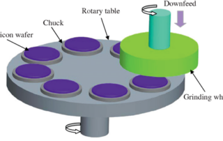
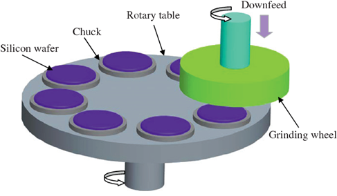
Wafer backgrinding is the first step in semiconductor packaging, the process of encasing one or more discrete semiconductor devices or integrated circuits (IC) for protection. Known also as wafer thinning or wafer lapping, backgrinding reduces wafer thickness to allow stacking and high-density IC packaging. Wafer thickness also determines package height, an important consideration as smartphones, laptops, and other electronic devices become thinner. With MEMS, wafer thinning also controls the proof mass for devices such as accelerometers or the diaphragm thickness for pressure sensors. Etching the surface of the wafer produces the IC but grinding the backside is what produces [...]