 Skip to content
Blogs
Two Ways to Measure EV Battery Plate Thickness
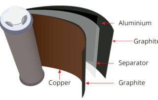
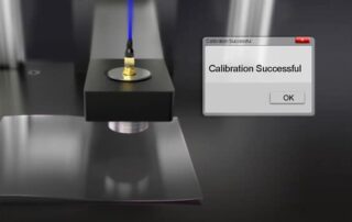
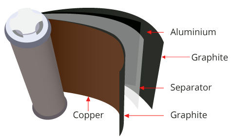
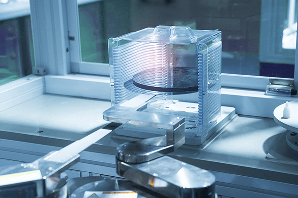
Two Ways to Measure EV Battery Plate Thickness Animation showing a system setup used to measure the thickness of thin conductive films such as electric vehicle (EV) battery electrodes. Description Learn how to measure EV battery plate thickness with MTI’s Digital Accumeasure, a high-precision capacitance measurement system with nanometer accuracy and stability. Problem Lithium battery plates for electric vehicles consist of lithium ion compounds applied to either a copper plate substrate (cathode plate) or an aluminum substrate (anode plate). The plates are approximately 100-200 um thick ( .004 - .008 inch). [...]
WAFER QA/QC AFTER SLICING AND POLISHING
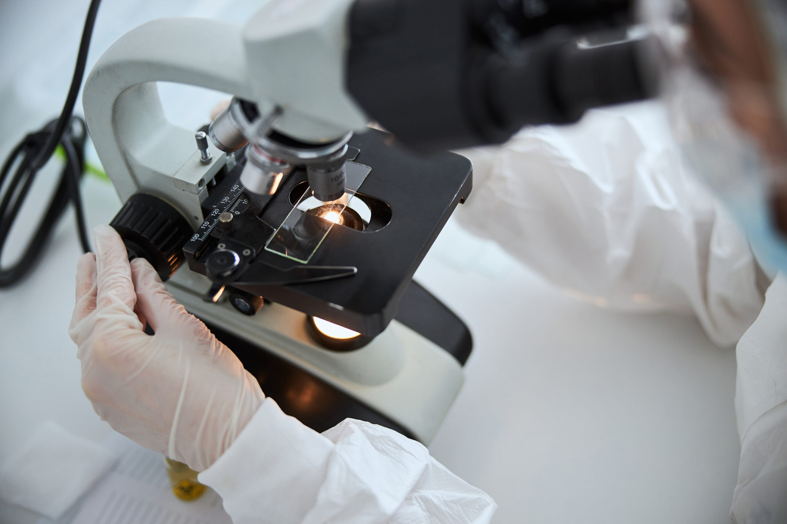
Industry Semiconductor Applications Wafer Qa/Qc After Slicing And Polishing Measurement Type Surface Description When wafers are sliced up with wire saws, they are measured to make sure they are within the specified thickness, with minimal bow, warp, and TTV. After initial measurement, they are sorted and sent for polishing. Since polishing removes material and smoothes out the rough surfaces they need to be measured again to ensure they meet thickness guidelines and quality standards. Solution: MTI Instruments manufactures multiple systems to perform thickness measurements. From semi automated Proforma 300SA to manual wafer [...]
Dynamic Measurement of Small Oscillatory Motions
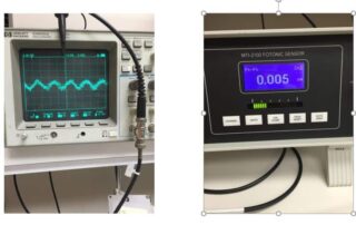
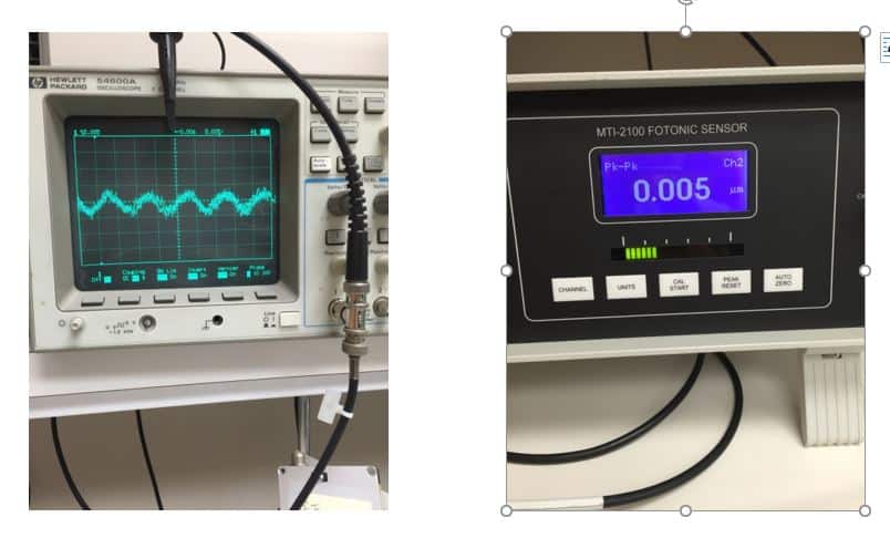
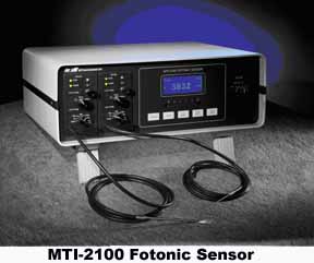
Dynamic Measurement of Small Oscillatory Motions Research & Development Piezoelectric Stack Motion Fotonic Systems Displacement Description This application note describes the measurement of a very small oscillatory motions (nanometers) produced by a piezo electric device with the MTI-2100 and the MTI-2032RX high-resolution module. Fotonic™ sensors from MTI Instruments are ideal for making dynamic measurements of very small oscillatory motions. Using the MTI-2100 Fotonic Sensor with a spectrum analyzer, angstrom level measurements are possible. Would you like to know more? Okay, let's set up some basic equipment and get started. Piezo [...]
ABOUT WAFER BOW AND WARP MEASUREMENT SYSTEMS
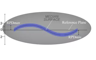
Thickness Measurement for Metrology Systems ASTM F657: The distance through a wafer between corresponding points on the front and back surface. Thickness is expressed in microns or mils (thousandths of an inch). Total Thickness Variation (TTV) ASTM F657: The difference between the maximum and minimum values of thickness encountered during a scan pattern or series of point measurements. TTV is expressed in microns or mils (thousandths of an inch). ASTM F534 3.1.2: The deviation of the center point of the median surface of a free, unclamped wafer from the median [...]
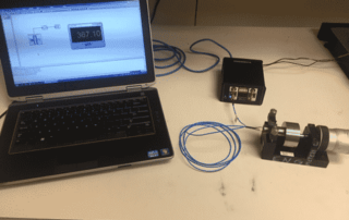
Interfacing MTI’s Digital Accumeasure to Measurement Computing’s DASYLab with Modbus
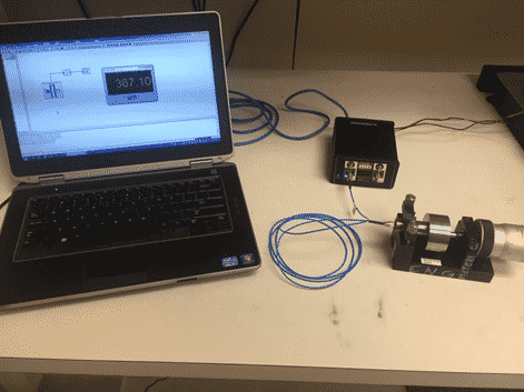
Interfacing MTI's Digital Accumeasure to Measurement Computing's DASYLab with Modbus Interfacing MTI's Digital Accumeasure to Measurement Computing's DASYLab with Modbus Displacement Description Laptop running MC DASYLab1 © and MTI Digital Capacitance sensor over Modbus TCP/IP Measurement Computing's DASYLab data acquisition software is easy to use and allows measuring with multiple system sensors (analog and digital). You can plot the results of multiple sensors versus time or encoder position and store the data with DASYLab. This application note describes how to interface MTI's Digital Capacitance Sensor over Ethernet TCP/IP. The DASYLab Modbus [...]
Displacement Measurement by Fiber Optics
Displacement Measurement by Fiber Optics Semiconductor, Research & Development 3D IC Construction Displacement, Vibration Description The Fotonic™ Sensor is a non-contact instrument which uses the fiber optics lever¬π principle to perform displacement, vibration and surface-condition measurements (Figure 1). The Fotonic Sensor transmits a beam of light through a flexible fiber-optic probe, receives light reflected from a target surface, and converts it into an electrical signal proportional to the distance between the probe tip and the target being measured.¬† The output signal voltage from the fiber optic sensor is then used [...]
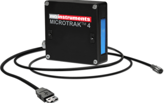
MicroTrak 4 Over a LAN for Ethernet Signaling
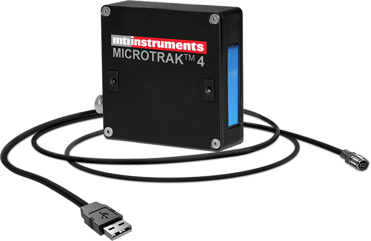
MicroTrak 4 Over a LAN for Ethernet Signaling Semiconductor, Research & Development 3D IC Construction Distance, Positioning, Displacement Description The MicroTrak 4, which is a USB device, can also be used over a LAN or even CAT 5e/6/7 wiring with additional hardware to convert the USB sensor to Ethernet signaling. The devices required to run over the LAN or direct CAT wire are Icron USB 2.0 Ranger 2301GE-LAN extender system. The MicroTtrak 4 basic software then runs on the host computer.  The LAN does not have to be dedicated; it [...]
LITHOGRAPHY OPTICS POSITION FOCUS
Industry Semiconductor Applications Photolithography Using Capacitance Sensors Measurement Type Positioning Description One specific area where capacitance systems excel is high resolution focusing of complex lens systems such as those found in atomic force microscopes, vision inspection machines and photolithography tools. In a multi-million dollar photolithography tool, high accuracy, nanometer resolution and maximum thermal stability are absolutely critical to maintain proper focus and obtain integrated circuit line widths as small as 45 nanometers. Additionally, most systems demand low power consumption and maximum heat dissipation to eliminate any adverse affects from [...]

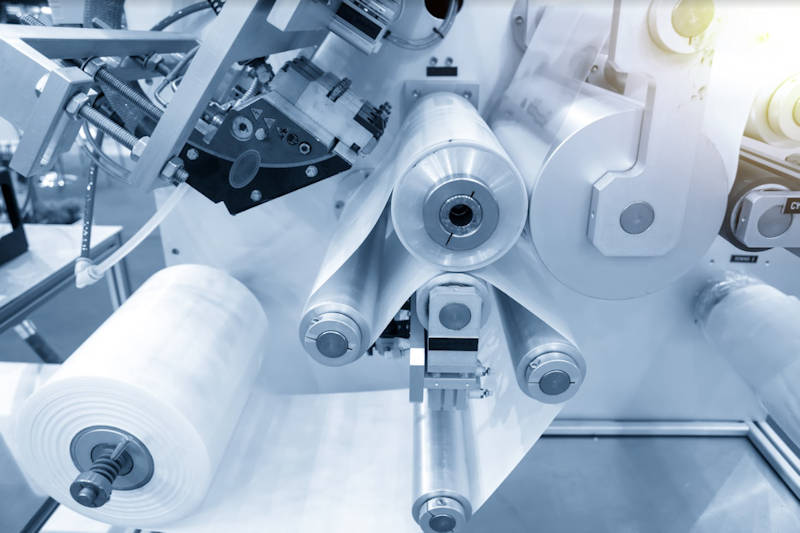
Monitor Roller Gaps and Parallelism
Monitor Roller Gaps and Parallelism Industrial Printing, Calendering, Crushing Gap Easy Roller Gap Measurement Ensures Calendering Success Many roll-to-roll finishing processes typically use a calender, or series of hard pressure rollers, to deliver smooth, high-quality products of plastic, textile, or paper (Fig 1). Ensuring a consistent material thickness, however, depends on the ability to monitor, and maintain, a precise gap between rollers. This application note describes a quick and easy means for roller gap measurement. Figure 1: Calender Rollers where consistent gap across the rollers are vital [...]
GAAS SUBSTRATE THICKNESS MEASUREMENT
Industry Semiconductor Applications Gaas Substrate Thickness Measurement Measurement Type Thickness Description Measuring Thickness of Wafers with Different Chemistries Introduction: Silicon wafers are ordinarily highly conductive and easy to measure with standard capacitive displacement sensors (See MTI’s Proforma 300i). Measuring the thickness of GaAs wafers that have high bulk resistivity (>10k Ohm/cm) is a little more difficult because the wafers act as non-conductive insulators in a capacitive sensor’s measuring field. Fortunately, MTI has a solution to this problem. Solution: It’s possible to measure the thickness and TTV of high resistivity semiconducting wafers (like GaAs) using non-contact capacitive [...]