 Skip to content
Blogs
 Five Common Mistakes with Semiconductor Wafer Measurement Gallery
Five Common Mistakes with Semiconductor Wafer Measurement
Application Notes-MTI, Brand-MTI, Industry-Compliance Testing, Industry-Consumer Products, Industry-Electronics, Industry-Manufacturing, Industry-Semiconductor, Industry-Semiconductor-MTI, Z-REPUB, z1
Five Common Mistakes with Semiconductor Wafer Measurement
Semiconductor wafer measurement requires a high degree of precision. The right metrology equipment and inspection processes are important, but so is procedural consistency and attention to detail. If you’re not getting the results you want, it’s time to look beyond the measurements. With bare semiconductor wafers, users need to avoid these five common mistakes. Mistake #1 | Turning the Device Off Most users turn on metrology devices only when it’s time to use them. As soon as semiconductor wafer measurement is complete, the devices are turned off. This reduces electricity consumption but also introduces thermal instability that can cause [...]
 Proforma 300i SA Video Shows Semiconductor Metrology Gallery
Proforma 300i SA Video Shows Semiconductor Metrology
Brand-MTI, Industry-Compliance Testing, Industry-Consumer Products, Industry-Electronics, Industry-Manufacturing, Industry-R&D, Industry-Semiconductor, Industry-Semiconductor-MTI, News-MTI-Metrology, News-Product Updates, Press Releases-Vitrek, Products-MTI-Semiconductor/Metrology, Videos-MTI, Videos-MTI-Manual Semiconductor Metrology System, Z-REPUB, z1
Proforma 300i SA Video Shows Semiconductor Metrology
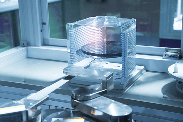
MTI Instruments, a worldwide leader in precision measurement solutions, has released a YouTube video that shows how its Proforma™ 300i SA semi-automated measurement tool measures silicon carbide wafers for semiconductors. George Relan, MTI’s Global Director of Sales, demonstrates how the desktop metrology system provides non-contact full wafer scanning and 3D mapping of measurement features such as thickness and shape. MTI’s video also shows how the Proforma 300i SA interfaces with an external computer and provides powerful Windows-based software for analysis and reporting. By utilizing MTI push/pull technology, the Proforma 300i SA doesn’t require the semiconductor wafers to have a [...]
 3D Integrated Circuits Use Capacitive Sensing to Ensure Coplanarity Gallery
3D Integrated Circuits Use Capacitive Sensing to Ensure Coplanarity
Application Notes-MTI, Brand-MTI, Industry-Consumer Products, Industry-Electronics, Industry-Manufacturing, Industry-Semiconductor, Industry-Semiconductor-MTI, Industry-Sensors, Z-REPUB, z1
3D Integrated Circuits Use Capacitive Sensing to Ensure Coplanarity
Three-dimensional (3D) integrated circuits (ICs) feature silicon wafers and dies that are stacked vertically for improved device performance. By using the Z-axis, 3D ICs can overcome the power and footprint limitations associated with two-dimensional (2D) integrated circuits. Yet 3D ICs need coplanar surfaces to contact all of the pads, pins, and pillars. To determine coplanarity, semiconductor manufacturers measure the angle and gap between two planes. Bonding tool actuators use these measurements to adjust components and ensure that all device pins and solder balls reside on the same geometric plane. This process, active parallelism compensation, promotes proper bonding without residual [...]
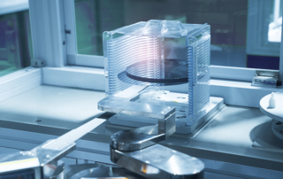
About Wafer Bow And Warp Measurement Systems
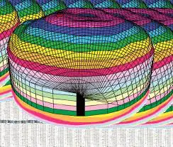
Semiconductor/Solar Wafer Bow And Warp Metrology/Surface About Wafer Bow And Warp Measurement Systems Thickness Measurement for Metrology Systems ASTM F657: The distance through a wafer between corresponding points on the front and back surface. Thickness is expressed in microns or mils (thousandths of an inch). Total Thickness Variation (TTV) ASTM F657: The difference between the maximum and minimum values of thickness encountered during a scan pattern or series of point measurements. TTV is expressed in microns or mils (thousandths of an inch). Figure above shows a wafer placed between two non-contact [...]
Laser Thickness Gauge System Principles
Microtrak™ 3 TGS The Microtrak™ 3 TGS system is specifically designed for thickness applications utilizing two lasers. The product can be used in a standalone configuration or easily interfaced with PLCs and PCs. Each module contains an integral LCD display and keypad for setup and display of measurements. A USB serial port also allows control by a laptop computer. Basic PLC or control input/output is provided by discrete digital I/O lines or a Modbus® interface. Laser Triangulation Principle The Microtrak™ 3 TGS system uses the principle of laser triangulation to perform a one dimensional [...]

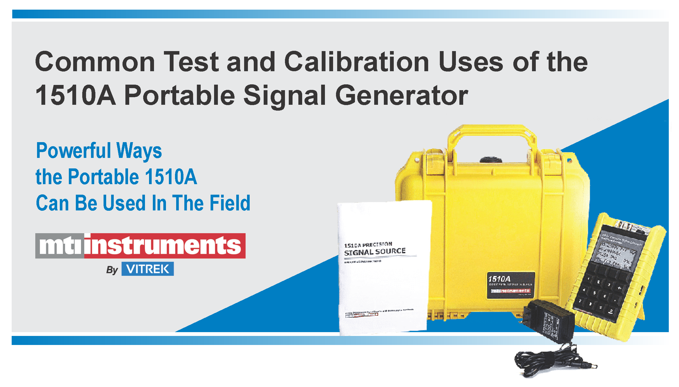
Common Test and Calibration Uses of the 1510A Portable Signal Generator
Introduction As one of the most versatile and powerful hand-held signal generators on the market, the 1510A is a two-channel, battery-powered, microprocessor-controlled direct digital signal generator. It has an average battery life of 3 hours of continuous use. Weighing in at under two pounds, makes it ideal for use in the field. There are many different ways this sophisticated device can be leveraged to perform precise test and calibration of equipment, wires, cables, sensors and much more. Use Case #1 | Sensor Simulation You can simulate sensors during system development, bring-up, and test. Often during [...]
Download How to Reduce Inconsistent Wafer Measurements
Thank you for downloading! Here's the link to How to Reduce Inconsistent Wafer Measurements.
Capacitance Guide for Industrial Applications
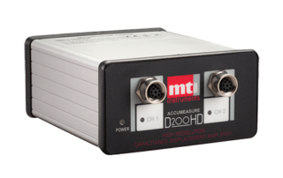
Accumeasure Digital Capacitance System D Series Gen 3 View Product Capacitance Displacement and Gap Measurement Probes View Product Accumeasure Analog Capacitance System View Product Basic Principles Capacitance is the ratio of the change in an electric charge to the corresponding change in its electrical potential (i.e., voltage). Capacitors, components that that have the “capacity” to store an electric charge, consist of conductive parallel plates that don’t touch or connect with each other. Instead, these metal plates are electrically-separated by air or a layer of insulating material (i.e., the dielectric). MTI’s technology [...]
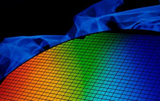
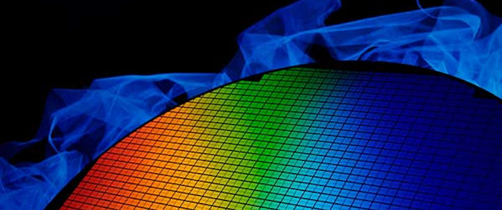
Increase SiC Wafer Production Yield
Demand for SiC wafers is growing rapidly and production needs to keep up. Speeding up production can result in higher defect rates without the proper inspection equipment in place during the R&D process, where poor verification of your process tools can dramatically reduce yield. MTI Instruments 300iSA system can help measure TTV, flatness, bow and warp of up to 20 wafers per hour. Our solution helps you perform wafer inspection verifications at scale and increases the throughput of your production yield as the demand grows for 100-200mm diameter wafers. Finding defects at volume can be difficult, but MTI’s superior [...]
Product Education & Training
Education & Training Vibration Measurement & Engine Rotor Balancing High-Speed Data Acquisition Products for Streaming Applications Industry Application Webinars Test & Measurement Solutions for Semiconductor Manufacturers GaGe Digitizers in Ultrasonic Applications Electrical Safety & Compliance Testing for Printed Circuit Board Manufacturers Vitrek Products for Metrologists & Calibration Labs Vitrek Electrical Safety Testing for the Appliance & Consumer Product Industries Compliance Testing for the Lighting Industry Webinar Vitrek [...]