 Skip to content
Blogs
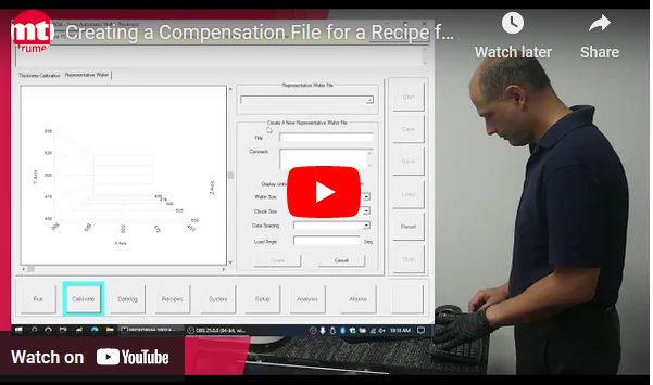
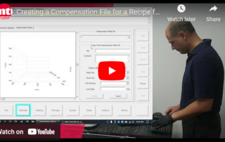 Creating a Compensation File for a Recipe for the Proforma 300iSA – Video Gallery
Creating a Compensation File for a Recipe for the Proforma 300iSA – Video
Brand-MTI, Industry-Compliance Testing, Industry-Electronics, Industry-Manufacturing, Industry-Semiconductor, Industry-Semiconductor-MTI, Industry-Semiconductor-Videos, News-MTI-Metrology, Products-MTI-Semiconductor/Metrology, Videos-MTI-Manual Semiconductor Metrology System, Videos-MTI-Semiautomated Metrology System, z1
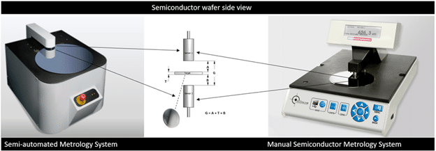
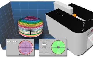 The Benefits of Manual, Semi-Automated, and Fully-Automated Systems for Semiconductor Wafer Inspection and Metrology Gallery
The Benefits of Manual, Semi-Automated, and Fully-Automated Systems for Semiconductor Wafer Inspection and Metrology
Application Notes-MTI, Brand-MTI, Industry-Consumer Products, Industry-Electronics, Industry-Manufacturing, Industry-Semiconductor, Industry-Semiconductor-MTI, News-MTI-Metrology, Products-MTI-Semiconductor/Metrology, z1
The Benefits of Manual, Semi-Automated, and Fully-Automated Systems for Semiconductor Wafer Inspection and Metrology
This is the third of three articles in Semiconductor Wafer Measurement for Increased Profitability. The first article in this series explains why disc geometry matters. The second article examines the cost of failing to inspect semiconductor wafers. Fully automated systems that can load, scan, and unload wafers are fast, convenient, and efficient at high volumes. They’re useful for checking every wafer in every batch, but these systems are expensive. Semi-automated and manual systems cost significantly less and are generally used for lower volumes; however, they’re also easy-to-use and can make fast, accurate measurements that support production flow. Semi-automated and [...]
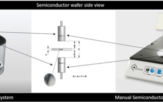 Why Disc Geometry Matters In Wafer Production Gallery
Why Disc Geometry Matters In Wafer Production
Application Notes-MTI, Brand-MTI, Industry-Consumer Products, Industry-Electronics, Industry-Manufacturing, Industry-Semiconductor, Industry-Semiconductor-MTI, News-MTI-Metrology, Products-MTI-Semiconductor/Metrology, z1
Why Disc Geometry Matters In Wafer Production
This is the first of three articles in Semiconductor Wafer Measurement for Increased Profitability. The second article examines the cost of failing to inspect semiconductor wafers. The third article describes the benefits of using semi-automated, fully-automated, and manual systems for wafer metrology and inspection. Semiconductor wafers are cut from cylindrical silicon crystals, or ingots. The flatness of these disc-shaped wafers is controlled to tight tolerances to ensure that the entire wafer surface is suitable for integrated circuit (IC) production. If disc geometry is out-of-spec after cutting, it may be possible to reprocess the wafer. Cutting is only the first [...]

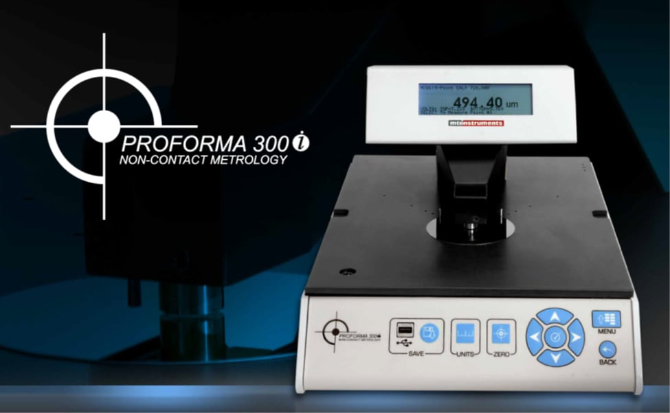
Measuring Glass wafer thickness with a Proforma 300i
Measuring glass substrate thickness with a Proforma 300i Semiconductor Glass Wafer Thickness Measurement Thickness Applications testing of glass (substrate) thickness An applications experiment was made with the MTI Proforma 300i Semiconductor thickness system to determine if it’s useful to measure glass substrate thicknesses typically found as support structures for Si semiconductors that are used for fabricating MEMs components and other thin Si wafers. The MEMs Silicon wafer is so thin after grinding that it needs the support of a thicker substrate to prevent breakage of the wafer during the back grinding/thinning [...]
 Advantages of Measuring Semiconductor Thin Film Thickness with Capacitance Gallery
Advantages of Measuring Semiconductor Thin Film Thickness with Capacitance
Application Notes-MTI, Brand-MTI, Industry-Compliance Testing, Industry-Electronics, Industry-Manufacturing, Industry-R&D, Industry-Semiconductor, Industry-Semiconductor-MTI, Industry-Sensors, Products-MTI-Capacitance, Products-MTI-Laser/Fiber Optic, Products-MTI-Semiconductor/Metrology, Z-REPUB, z1
Advantages of Measuring Semiconductor Thin Film Thickness with Capacitance
Semiconductor Thin Films: Measuring Thickness with Capacitance In the semiconductor industry, thin films are deposited onto silicon and other wafer materials one atomic layer at a time. The thickness of these extremely thin coatings is important because thin-film thickness affects the wafer’s electrical, optical, and mechanical properties. With semiconductors, either conductive metallic films or non-conductive metal oxide films are deposited. There are two main thin-film coating methods, chemical vapor deposition (CVD) and physical vapor deposition (PVD), both of which use a variety of processes. Because the coatings for semiconductor wafers are so thin, thickness measurement require a high degree [...]
 Contact vs. Non-Contact Measurement and Linear Displacement Sensors Gallery
Contact vs. Non-Contact Measurement and Linear Displacement Sensors
Application Notes-MTI, Brand-MTI, Industry-Compliance Testing, Industry-Consumer Products, Industry-Electronics, Industry-Manufacturing, Industry-Semiconductor, Industry-Semiconductor-MTI, Industry-Sensors, Products-MTI-Capacitance, Z-REPUB, z1, ZOK
Contact vs. Non-Contact Measurement and Linear Displacement Sensors
Contact vs. Non-Contact Measurement and Linear Displacement Sensors Linear displacement sensors are used to measure the distance between two points or two plane surfaces. They use various technologies, but there are two basic types: contact and non-contact. As their names suggest, contact sensors make physical contact with the object that is being measured and non-contact sensors do not. This is an obvious but important difference, but there is much more to consider. Non-contact measurement is faster than contact measurement, especially for applications with high sampling rates. Because contact-type devices must touch and then traverse the object, measurement is slower. [...]
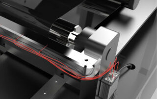
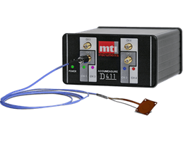
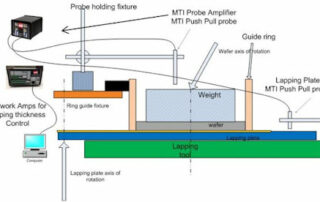
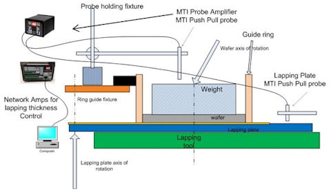
Semiconductor Wafer Lapping and Displacement Measurement
Semiconductor Wafer Lapping and Displacement Measurement Semiconductor Semiconductor Wafer Manufacturing Displacement Description Semiconductor Wafer Lapping and Displacement Measurement This application note explains how MTI’s Accumeasure technology was used with a lapping machine to measure displacement (wafer material removal) and determine the new semiconductor wafer thickness. Changes in electrical capacitance (displacement) were measured and then directly converted into a 24-bit digital reading to obtain precise digital thickness measurements. During lapping, a wafer of known start thickness is placed on a rotary lapping table. The backside of the wafer faces downward and [...]