 Skip to content
Blogs
GaAs Substrate Thickness Measurement
GaAs Substrate Thickness Measurement Semiconductor Gaas Substrate Thickness Measurement Thickness Description Measuring Thickness of Wafers with Different Chemistries Introduction:  Silicon wafers are ordinarily highly conductive and easy to measure with standard capacitive displacement sensors (See MTI's Proforma 300i). Measuring the thickness of GaAs wafers that have high bulk resistivity (>10k Ohm/cm) is a little more difficult because the wafers act as non-conductive insulators in a capacitive sensor's measuring field. Fortunately, MTI has a solution to this problem. Solution:  It’s possible to measure the thickness and TTV of high resistivity semiconducting [...]

Hard Drive Position
Semiconductor Hard Drive Position Positioning Description
LED Substrate Thickness
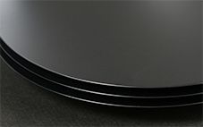
LED Substrate Thickness Semiconductor Led Substrate Thickness Thickness Description Remember that old acronym, GIGO?  Garbage in garbage out, it can apply to raw materials as well as programming. Sapphire wafers need to be of a certain quality to ensure maximum yield. Excessive TTV, Bow, and Warp lead to premature LED failure. LED manufacturers need to inspect incoming wafers. Wafer producers also need to check and control TTV, Bow and Warp. The market for sapphire wafers, driven by the growth in LED manufacturing, is booming. While the price has come down [...]

Photolithography Using Capacitance Sensors
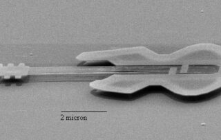
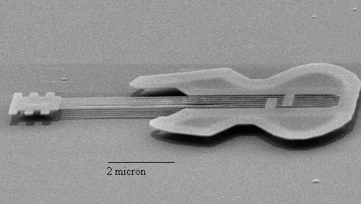
Photolithography Using Capacitance Sensors Semiconductor Photolithography Using Capacitance Sensors Positioning Description When it comes to photolithography, how accurate are our sensors? Accurate enough to measure this: ​   Photo by D. Carr and H. Craighead, Cornell The world's smallest guitar is 10 micrometers long -- about the size of a single cell -- with six strings each about 50 nanometers, or 100 atoms, wide. Made by Cornell University researchers from crystalline silicon, it demonstrates a new technology for a new generation of electromechanical devices. Even the world’s smallest guitar’s 2 [...]
MTI Video: Wafer Inspection & Metrology Startup (Proforma 300iSA)
https://youtu.be/mawagL6Yg3U
MTI Video: Wafer Inspection and Metrology Tutorial (Proforma 300i)
https://www.youtube.com/watch?v=nGkbpG2sz_k Learn More Download this brochure to learn more about the Proforma 300i wafer measurement system for semiconducting and semi-insulating wafers. This article in AZO Sensors also provides information.
New Video from MTI! Closed-loop System to Monitor and Control Conductive Film Thickness During Manufacturing
Closed-loop System to Monitor and Control Conductive Film Thickness During Manufacturing This animation demonstrates how Accumeasure with capacitance probes can be used as a solution to measure and control conductive film thickness in a production line where these measurements can be fed back to a controller which adjusts the roller(s) to increase or decrease the gap to keep the film’s thickness within specification. The MTI Instruments Capacitive system has greater than 100 nm resolution and 1um accuracy. This solution is appropriate for measuring the following: EV battery plate thickness Non-woven conductive material thickness Conductive film thickness Roll-to-roll conductive [...]
WAFER MEASUREMENT – UNGROUNDED
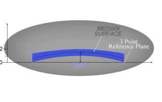
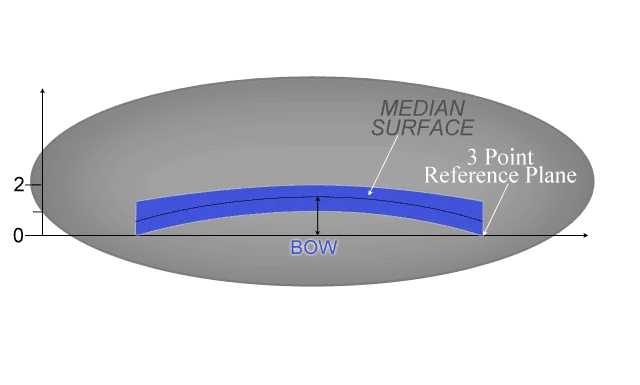
Industry Semiconductor Applications Wafer Measurement – Ungrounded Measurement Type Metrology Description MTI Instruments Inc. has developed a thickness measurement device that eliminates the effect of varying target conductivity. Called the Push-Pull probe, it’s a unique version of the AccumeasureTM amplifier series. This special design provides accurate surface information for wafer bow and warp. Bow is the deviation of the center point of the median surface of a free, un-clamped wafer from the median surface to the reference plane. Where, the reference plane is defined by three corners of equilateral triangle. This [...]
PHOTOLITHOGRAPHY USING CAPACITANCE SENSORS
Industry Semiconductor Applications Lithography Optics Position Focus Measurement Type Positioning Description When it comes to photolithography, how accurate are our sensors? Photo by D. Carr and H. Craighead, Cornell - The world’s smallest guitar is 10 micrometers long — about the size of a single cell — with six strings each about 50 nanometers, or 100 atoms, wide. Made by Cornell University researchers from crystalline silicon, it demonstrates a new technology for a new generation of electromechanical devices. Even the world’s smallest guitar’s 2 micron [...]
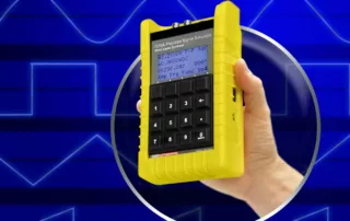
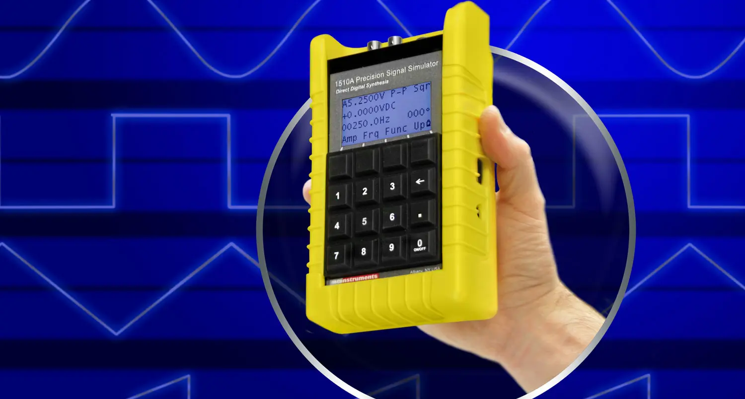
High Precision Portable Signal Generators and Calibrators: Everything You Need to Know
High precision portable signal generators are portable electronic devices that generate highly precise signals for testing, system calibration, sensor simulation, troubleshooting, and monitoring. Unlike the benchtop signal generators that are used in laboratories, these hand-held portable devices are designed to be used in the field. The best high precision portable signal generators are also rugged and NIST traceable, meaning that their manufacturer calibrates them to standards from the National Institute of Standards and Technology (NIST). In terms of cost, high precision portable signal generators are more expensive than less precise, lower-end devices that can be held in the hand; [...]