 Skip to content
Blogs
About Wafer Bow And Warp Measurement Systems
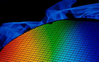
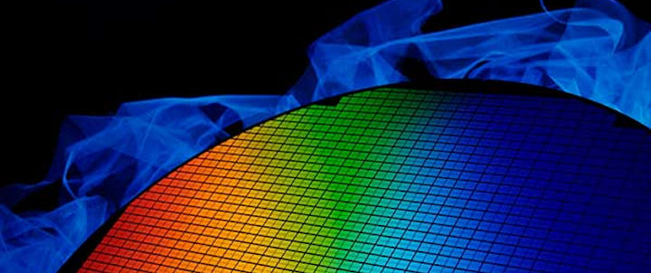
Semiconductor/Solar Wafer Bow And Warp Metrology/Surface About Wafer Bow And Warp Measurement Systems Thickness Measurement for Metrology Systems ASTM F657: The distance through a wafer between corresponding points on the front and back surface. Thickness is expressed in microns or mils (thousandths of an inch). Total Thickness Variation (TTV) ASTM F657: The difference between the maximum and minimum values of thickness encountered during a scan pattern or series of point measurements. TTV is expressed in microns or mils (thousandths of an inch). Figure above shows a wafer placed between two non-contact [...]