 Skip to content
Blogs
 EV Batteries Need Thickness Gauging for Lower Costs and Higher Performance Gallery
EV Batteries Need Thickness Gauging for Lower Costs and Higher Performance
Application Notes-MTI, Brand-MTI, Industry-Automotive, Industry-Compliance Testing, Industry-Consumer Products, Industry-Electronics, Industry-Manufacturing, Industry: Transportation, News-MTI, Products-MTI, Products-MTI-Capacitance, Products-MTI-Laser/Fiber Optic, Z-REPUB, z1
EV Batteries Need Thickness Gauging for Lower Costs and Higher Performance
EV batteries need to cost less and last longer. Until the e-mobility industry solves these challenges, electric vehicle (EV) adoption won’t match the hype that’s driven by Tesla, the established automakers, and a host of startups who are attracting investors. According to Axios, the expense of owning an electric vehicle will exceed that of owning a conventional one until EV batteries cost less than $100/KWh to produce. Unfortunately, the EV industry isn’t expected to hit that target for another ten years. Yet, there is some encouraging news. Less expensive and better performing EV batteries are just a few years [...]
 High Resolution Semiconductor Wafer Measurements at Lower Costs Gallery
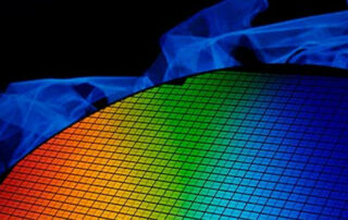
High Resolution Semiconductor Wafer Measurements at Lower Costs
Application Notes-MTI, Brand-MTI, Industry-Consumer Products, Industry-Electronics, Industry-Manufacturing, Industry-Semiconductor, Industry-Semiconductor-MTI, Products-MTI-Capacitance, Products-MTI-Semiconductor/Metrology, Z-REPUB, z1
High Resolution Semiconductor Wafer Measurements at Lower Costs
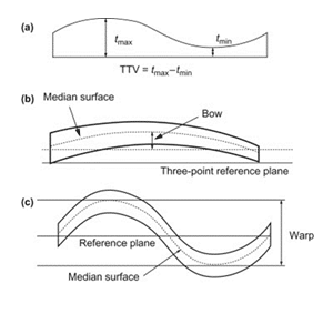
MTI's Proforma technology characterizes semiconductor wafers in terms of bow and warp, thickness, total thickness variation (TTV) and center thickness. Until recently, semiconductor wafer measurements at resolutions less than 100 µm were cost-prohibitive. Moreover, only expensive devices such as interferometers were capable of these measurements. Today, the semiconductor industry can use capacitance gauges instead of laser interferometers to achieve high resolution at fraction of the cost. Much like affordable CCD cameras transformed and expanded the market for video, cost-effective capacitance is disrupting the semiconductor wafer measurement market and creating new opportunities for quality testing and validation. The [...]
 Measure Wafer Bow, Warp and TTV with Capacitance Gallery
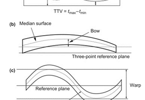
Measure Wafer Bow, Warp and TTV with Capacitance
Application Notes-MTI, Brand-MTI, Industry-Battery, Industry-Compliance Testing, Industry-Consumer Products, Industry-Electronics, Industry-Manufacturing, Industry-Semiconductor, Industry-Semiconductor-MTI, Industry-Sensors, Products-MTI-Capacitance, Z-REPUB, z1, ZOK
Measure Wafer Bow, Warp and TTV with Capacitance
The flatness of silicon wafers used to manufacture integrated circuits is controlled to tight tolerances to help ensure that the whole wafer is sufficiently flat for lithographic processing. To ensure your wafer manufacturing process is within tolerance, you need to measure the wafers being produced. Various measurement techniques exist to verify process tolerances and eliminate expensive scrap wafers. Non-contact capacitive sensing is a highly precise and cost-effective means to measure wafer flatness, bow, warp, and total thickness variation (TTV). MTI Instruments’ Proforma 300i and 300iSA systems use capacitance sensors to improve yields while reducing costs through better dimensional control of [...]
 How to Measure Dielectric Separator Thickness in EV Batteries Gallery
How to Measure Dielectric Separator Thickness in EV Batteries
Application Notes-MTI, Brand-MTI, Industry-Automotive, Industry-Compliance Testing, Industry-Consumer Products, Industry-Electronics, Industry-Government/Military, Industry-Manufacturing, Industry: Transportation, News-MTI, News-MTI-Instrumentation, Products-MTI-Capacitance, Products-MTI-Laser/Fiber Optic, Products-MTI-Signal Generators, Z-REPUB, z1
How to Measure Dielectric Separator Thickness in EV Batteries
The International Energy Agency predicts that as many as 125 million electric vehicles (EVs) will be on the road by 2030. At the heart of these electric cars, trucks, and buses is the lithium-ion (Li-ion) battery, a type of rechargeable battery with high energy density and low self-discharge. The plates in Li-ion batteries consist of lithium compounds that are applied to either a copper plate substrate (cathode) or an aluminum substrate (anode). In turn, these two plates are separated by a dielectric separator. All of the layers in an EV battery are extremely thin. In fact, the cathode and [...]
Capacitance Sensing for Non-Contact Thickness Measurements of Insulating Materials
Capacitance sensing can be used to make non-contact thickness measurements for most insulating materials. Capacitance sensors are known for their ability to precisely measure the thickness and position of conductive targets, but what’s less known is that these sensors can also measure the thickness of non-conductive materials. Examples include glass, sapphire, and plastics, as well as semi-insulating semiconductor materials such as GaAs and silicon nitride. Analog vs. Digital Technologies MTI Instruments, a global supplier of precision measurement technologies, takes the guesswork out of what used to be a complex measurement for non-conductive materials. MTI's Digital Accumeasure system features a [...]
 Trends in High Resolution Sensors for Semiconductor Metrology and Inspection Gallery
Trends in High Resolution Sensors for Semiconductor Metrology and Inspection
Application Notes-MTI, Brand-MTI, Industry-Compliance Testing, Industry-Consumer Products, Industry-Electronics, Industry-Manufacturing, Industry-Semiconductor, Industry-Semiconductor-MTI, Products-MTI-Capacitance, Products-MTI-Semiconductor/Metrology, Z-REPUB, z1
Trends in High Resolution Sensors for Semiconductor Metrology and Inspection
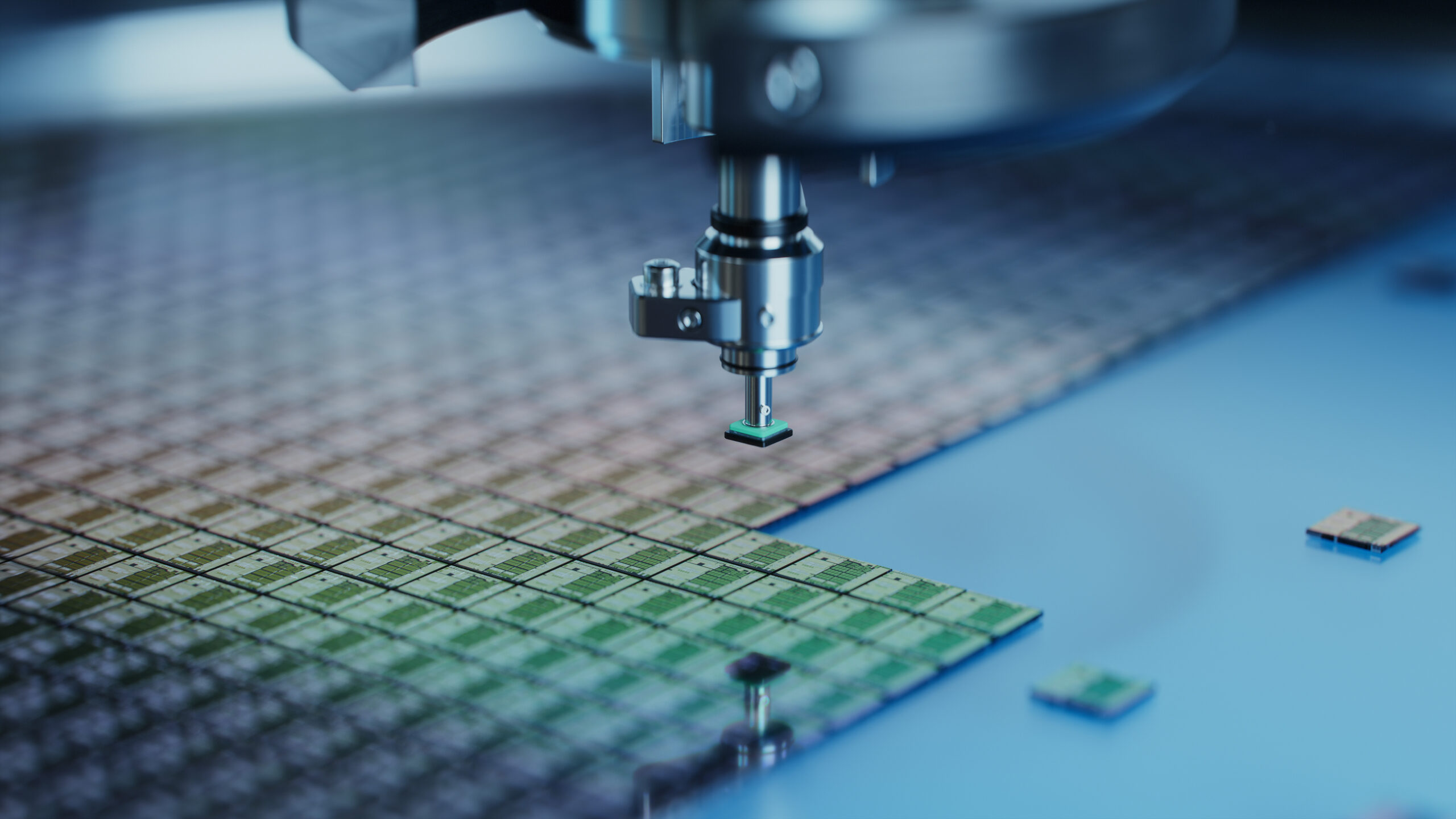
High resolution sensors are supporting improvements in semiconductor metrology and inspection at vital points in the production process. Because the fabrication of semiconductor wafers may require hundreds of steps and weeks of manufacturing time, early-stage defects that go undetected can have costly downstream consequences. Plus, because semiconductor processing always requires a high degree of precision, advances in fabrication methods seem to require ever-finer measurements in a never-ending quest. Today’s metrology instruments are incorporating high resolution sensors for automated wafer inspection. Resolution, the smallest measurement that a sensor can reliably indicate, may be given in dimensional units such as nanometers [...]
 White Paper: Precision Power Analyzers Gallery
White Paper: Precision Power Analyzers
Brand-Vitrek, Industry-Compliance Testing, Industry-Consumer Products, Industry-Electronics, Industry-Energy, Industry-Manufacturing, Industry-R&D, News-Product Updates, News-Products, News-Vitrek, Products-Vitrek-Power-Analyzer, Whitepapers-Vitrek, z1
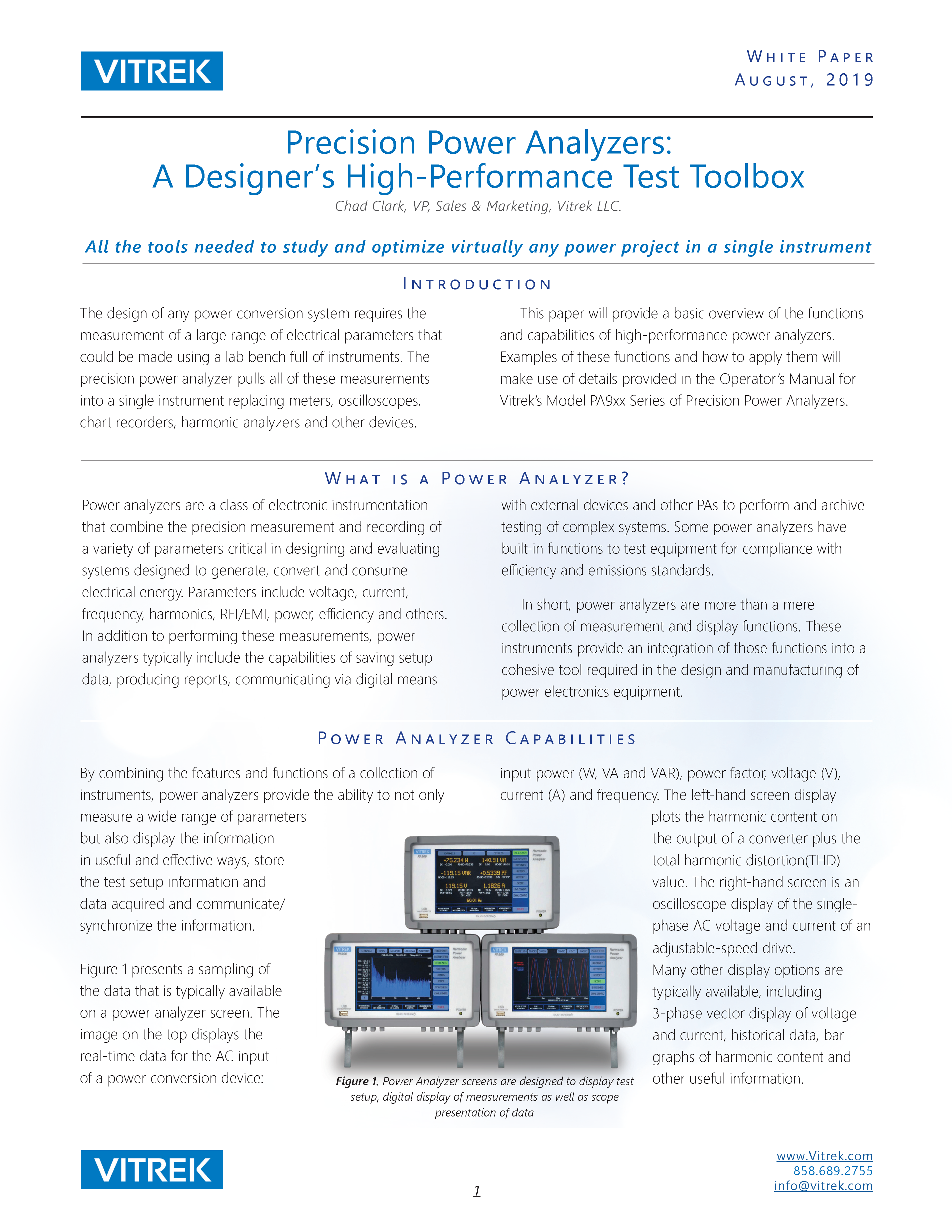
White Paper: Precision Power Analyzers
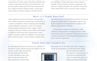
White Paper All the tools needed to study and optimize virtually any power project in a single instrument Introduction The design of any power conversion system requires the measurement of a large range of electrical parameters that could be made using a lab bench full of instruments. The precision power analyzer pulls all of these measurements into a single instrument replacing meters, oscilloscopes, chart recorders, harmonic analyzers and other devices. This paper will provide a basic overview of the functions and capabilities of high-performance power analyzers. Examples of these functions and how to apply [...]

How to Reduce Inconsistent Wafer Measurements
How to Reduce Inconsistent Wafer Measurements Avoid 5 Common Mistakes That Destroy Wafer Measurement Accuracy You take pride in your work. You’re precise, accurate and depend on the right metrology equipment. Then why are your bare semi-conductor wafer measurements sometimes inconsistent? It may be something you’re doing (or not doing) — without realizing it. MTI Instruments discovered there are five common mistakes that engineers and users make with bare semi-conductor wafers. The “Five Mistakes Made When Taking Semiconductor Wafer Measurements” Tech-Brief details these all-too-typical errors that adversely impact [...]
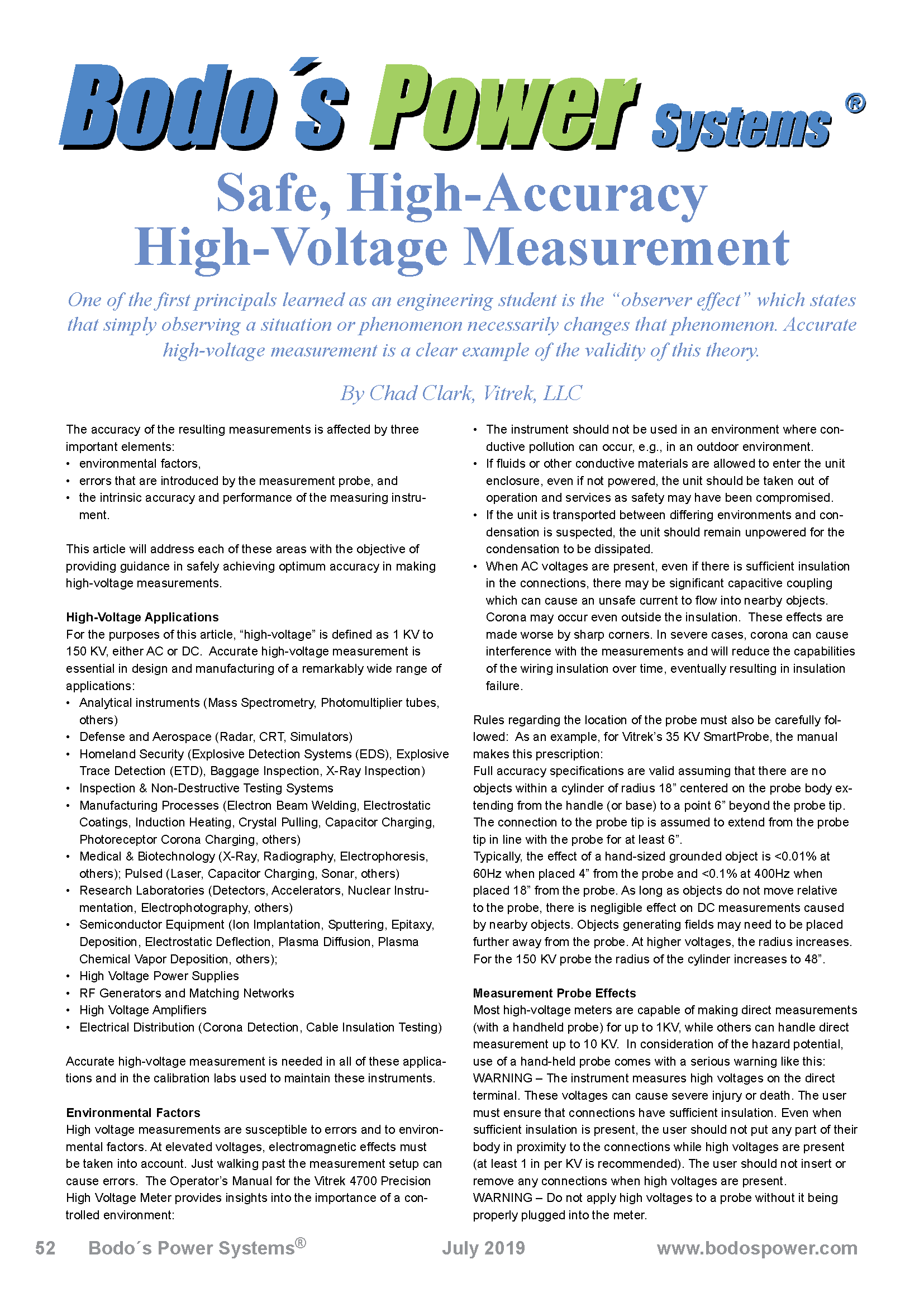
Vitrek featured in Bodo’s Power Systems
Click here to Download a copy of this article! Click here to Download a copy of this article!
 Five Common Mistakes with Semiconductor Wafer Measurement Gallery
Five Common Mistakes with Semiconductor Wafer Measurement
Application Notes-MTI, Brand-MTI, Industry-Compliance Testing, Industry-Consumer Products, Industry-Electronics, Industry-Manufacturing, Industry-Semiconductor, Industry-Semiconductor-MTI, Z-REPUB, z1
Five Common Mistakes with Semiconductor Wafer Measurement
Semiconductor wafer measurement requires a high degree of precision. The right metrology equipment and inspection processes are important, but so is procedural consistency and attention to detail. If you’re not getting the results you want, it’s time to look beyond the measurements. With bare semiconductor wafers, users need to avoid these five common mistakes. Mistake #1 | Turning the Device Off Most users turn on metrology devices only when it’s time to use them. As soon as semiconductor wafer measurement is complete, the devices are turned off. This reduces electricity consumption but also introduces thermal instability that can cause [...]