 Skip to content
Blogs
 Using Capacitance Sensors for Non-Conductive Material Measurement Gallery
Using Capacitance Sensors for Non-Conductive Material Measurement
Application Notes-MTI, Brand-MTI, Industry-Compliance Testing, Industry-Consumer Products, Industry-Electronics, Industry-Manufacturing, Industry-Sensors, News-MTI, News-MTI-Instrumentation, Products-MTI-Capacitance, Z-REPUB, z1
Using Capacitance Sensors for Non-Conductive Material Measurement
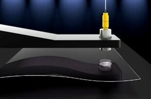
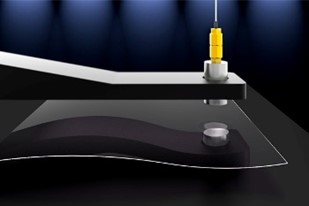
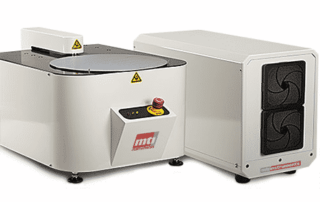
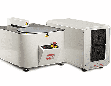
Non-Conductive Material Measurement with Capacitance Sensors Capacitance sensors are non-contact devices that can be used to obtain position, thickness, and dynamic measurements with a high degree of precision, accuracy, and resolution. Capacitive measurement is used with electrically-conductive materials such as metals but can also be used to measure non-conductive materials such as glass, sapphire, and many plastics. Even if a non-conductive material is relatively inexpensive (such as closed cell foam), manufacturers want to avoid errors that can result in significant waste across high volumes. Importantly, capacitance measurement is also used with semi-insulating materials such as gallium arsenide (GaAs) and [...]
 Why Demand for SiC Wafers is Hot and Durable Gallery
Why Demand for SiC Wafers is Hot and Durable
Brand-MTI, Industry-Consumer Products, Industry-Electronics, Industry-Manufacturing, Industry-Semiconductor, Industry-Semiconductor-MTI, MTI Blog, News-MTI, News-MTI-Metrology, Products-MTI-Semiconductor/Metrology, Z-REPUB, z1
Why Demand for SiC Wafers is Hot and Durable
Why Demand for SiC Wafers is Hot and Durable Pardon the pun, but SiC wafers are a hot item for high-temperature applications. Silicone carbide (SiC), a semiconductor containing both silicon and carbide, withstands temperatures up to 2700°C. Carborundum, as this durable ceramic is also known, finds additional applications in bulletproof vests, extrusion dies, sandpaper, and high-performance disc brakes. In electronics, SiC materials are used with light-emitting diodes (LEDs) and detectors. In the semiconductor industry, a market where interest is red-hot, SiC wafers are used in electronic devices that operate at high temperatures, high voltages, or both. Examples include electric [...]
Wafer Stress Analysis Using the 300iSA
Wafer Stress Analysis Using MTI Instruments Proforma 300iSAWafer processing involves several stages that may translate into mechanical alterations. Sometimes these alterations can cause deformities that render the wafer either unusable or that put it marginally close to not being usable. To determine this, stress analysis can be used.The Proforma 300iSA wafer characterization tool provides a software capability in which a wafer can be analyzed prior to processing and then after processing. The tool then evaluates how the wafer changed and hence, provides the resulting stress analysis.The software expects the customer to provide the material elasticity constants and to define them [...]
 CMP and Capacitance-Based Semiconductor Wafer Measurement Gallery
CMP and Capacitance-Based Semiconductor Wafer Measurement
Application Notes-MTI, Brand-MTI, Industry-Compliance Testing, Industry-Consumer Products, Industry-Electronics, Industry-Manufacturing, Industry-Semiconductor, Industry-Semiconductor-MTI, Industry-Sensors, Products-MTI-Capacitance, Products-MTI-Semiconductor/Metrology, z1
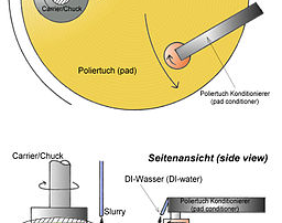
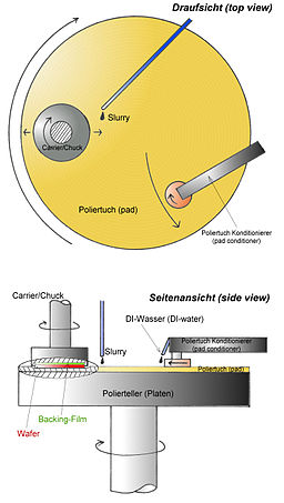
CMP and Capacitance-Based Semiconductor Wafer Measurement
Chemical mechanical polishing (CMP) uses chemical oxidation and mechanical abrasion to selectively remove material from semiconductor wafers in order to achieve very high levels of planarity. The planarity, or flatness, of these wafers is important for optical lithography, a microfabrication technique that produces integrated circuits (ICs) by transferring a geometric pattern from a photomask to a light-sensitive chemical photoresist. Also known as photolithography or UV lithography, optical lithography can produce a geometric pattern on a thin film or directly onto the substrate. Semiconductor Wafer Measurements: Flatness and Shape During optical lithography, variations in wafer flatness must be smaller than [...]
 MEMS and Capacitance-Based Semiconductor Wafer Measurement Gallery
MEMS and Capacitance-Based Semiconductor Wafer Measurement
Application Notes-MTI, Brand-MTI, Industry-Compliance Testing, Industry-Consumer Products, Industry-Electronics, Industry-Manufacturing, Industry-Semiconductor, Industry-Semiconductor-MTI, Industry-Sensors, Products-MTI-Capacitance, Products-MTI-Semiconductor/Metrology, Z-REPUB, z1
MEMS and Capacitance-Based Semiconductor Wafer Measurement
MEMS Technology and Capacitance-Based Wafer Measurement Micro-electrical-mechanical systems (MEMS) are tiny devices that house electrical and mechanical components on a single silicon chip or integrated circuit (IC). They integrate mechanical structures with electronics that are normally fabricated with complementary metal-oxide-semiconductor (CMOS) technologies. In addition to miniaturization, the benefits of MEMS include expanded functionalities at lower cost and with improved performance and reliability. With MEMS devices, critical physical dimensions range from smaller than one micron (µ) to larger than several millimeters (mm). In complex systems, multiple moving elements may be controlled by integrated electronics. Examples of the mechanical components in [...]
 Wafer Backgrinding and Semiconductor Thickness Measurements Gallery
Wafer Backgrinding and Semiconductor Thickness Measurements
Application Notes-MTI, Brand-MTI, Industry-Compliance Testing, Industry-Consumer Products, Industry-Electronics, Industry-Manufacturing, Industry-Semiconductor, Industry-Semiconductor-MTI, News-MTI-Instrumentation, News-MTI-Metrology, Products-MTI-Capacitance, Products-MTI-Semiconductor/Metrology, Z-REPUB, z1
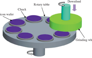
Wafer Backgrinding and Semiconductor Thickness Measurements
Wafer backgrinding is the first step in semiconductor packaging, the process of encasing one or more discrete semiconductor devices or integrated circuits (IC) for protection. Known also as wafer thinning or wafer lapping, backgrinding reduces wafer thickness to allow stacking and high-density IC packaging. Wafer thickness also determines package height, an important consideration as smartphones, laptops, and other electronic devices become thinner. With MEMS, wafer thinning also controls the proof mass for devices such as accelerometers or the diaphragm thickness for pressure sensors. Etching the surface of the wafer produces the IC but grinding the backside is what produces [...]
 Silicon Carbide vs. Silicon in EV Power Electronics Gallery
Silicon Carbide vs. Silicon in EV Power Electronics
Application Notes-MTI, Brand-MTI, Industry-Automotive, Industry-Battery, Industry-Compliance Testing, Industry-Consumer Products, Industry-Electronics, Industry-Government/Military, Industry-Manufacturing, Industry-R&D, News-MTI-Instrumentation, Products-MTI-Capacitance, Z-REPUB, z1
Silicon Carbide vs. Silicon in EV Power Electronics
Compare silicon carbide vs. silicon for electric vehicle (EV) power electronics and learn about SiC wafer measurement. As demand for electric vehicles (EVs) continues to grow, manufacturers are comparing two semiconductor technologies, silicon carbide and silicon, for power electronics applications. Silicon carbide (SiC) provides the high temperature resistance, low power consumption, rigidity, and support for smaller, thinner designs that EV power electronics need. Examples of SiC’s current applications include on-board DC/DC converters, off-board DC fast chargers, on-board battery chargers, EV powertrains, and automotive lighting for LEDs. According to Automotive World, SiC technology could also drive future EV innovations [...]
Film Sound Quality Control
Customer Case In performing quality control of the sound quality on film, the customer requires a fairly slow sampling and very high vertical resolution. Because the customer does not produce the actual film, there is a need to double-check the sound quality before it hits the theatres. Being sound, the highest frequency component is 20 KHz and they will probably oversample by a factor of 20. The customer would like to control the card via LabVIEW. GaGe Case Solution The CompuScope 1450 was suggested for its high resolution and ability to sample over a wide range of frequencies. Should [...]
 White Paper: Electrical Safety & Compliance Testing for Appliance & Consumer Product Manufacturers Gallery
White Paper: Electrical Safety & Compliance Testing for Appliance & Consumer Product Manufacturers
Brand-Vitrek, Industry-Compliance Testing, Industry-Consumer Products, Industry-Electronics, Industry-Manufacturing, News-Vitrek, Products-Vitrek, Whitepapers-Vitrek, z1
White Paper: Electrical Safety & Compliance Testing for Appliance & Consumer Product Manufacturers
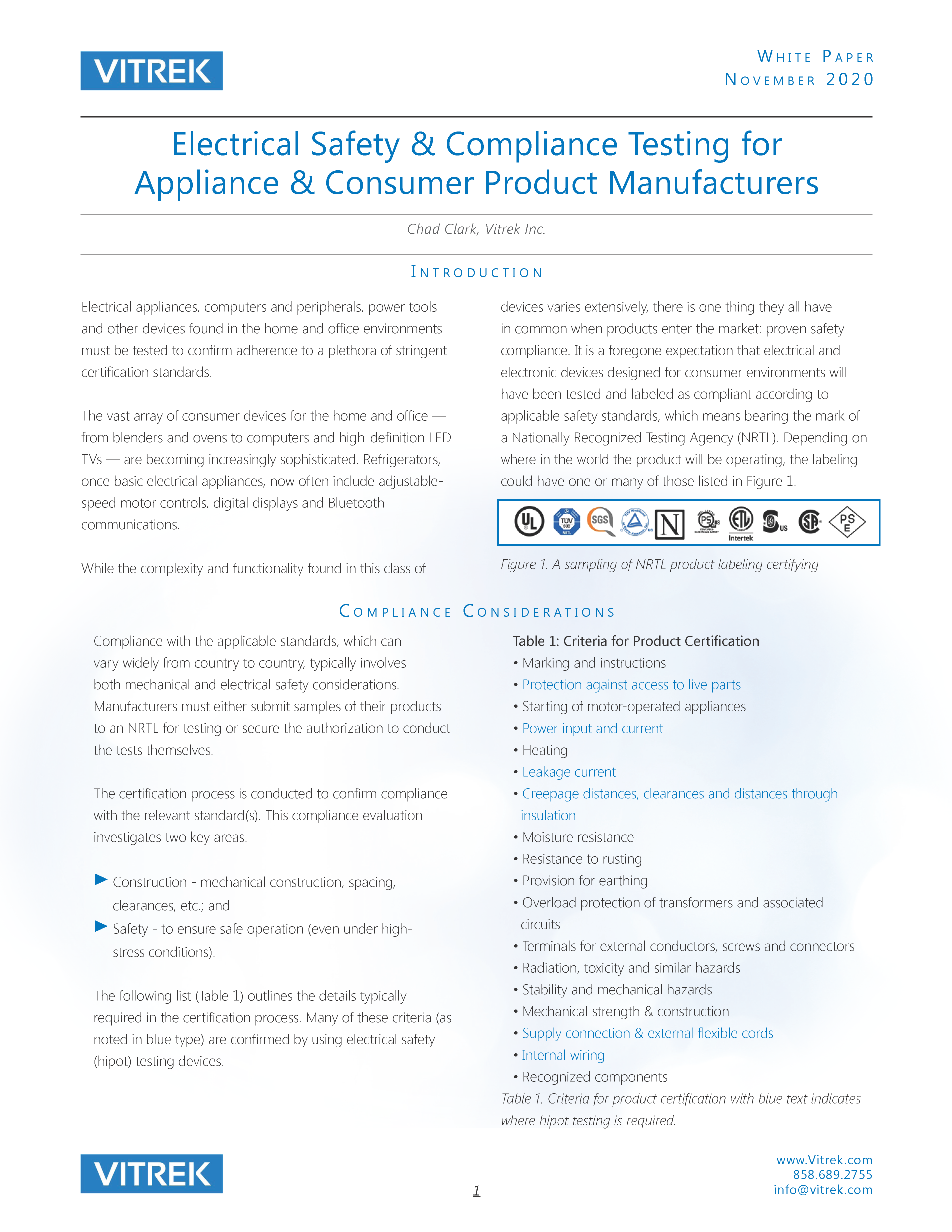
Introduction Electrical appliances, computers and peripherals, power tools and other devices found in the home and office environments must be tested to confirm adherence to a plethora of stringent certification standards. The vast array of consumer devices for the home and office — from blenders and ovens to computers and high-definition LED TVs — are becoming increasingly sophisticated. Refrigerators, once basic electrical appliances, now often include adjustable speed motor controls, digital displays and Bluetooth communications. While the complexity and functionality found in this class of devices varies extensively, there is one thing they all have in common when [...]
 Press Release: Vitrek Announces New SE Series High Voltage Safety Enclosures Gallery
Press Release: Vitrek Announces New SE Series High Voltage Safety Enclosures
Brand-Vitrek, Industry-Automotive, Industry-Cable Test, Industry-Compliance Testing, Industry-Consumer Products, Industry-Education, Industry-Electronics, Industry-Lighting, Industry-Manufacturing, News-Products, News-Vitrek, Press Releases-Vitrek, Products-Vitrek-Hipot, z1
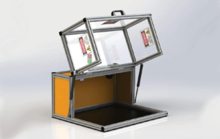
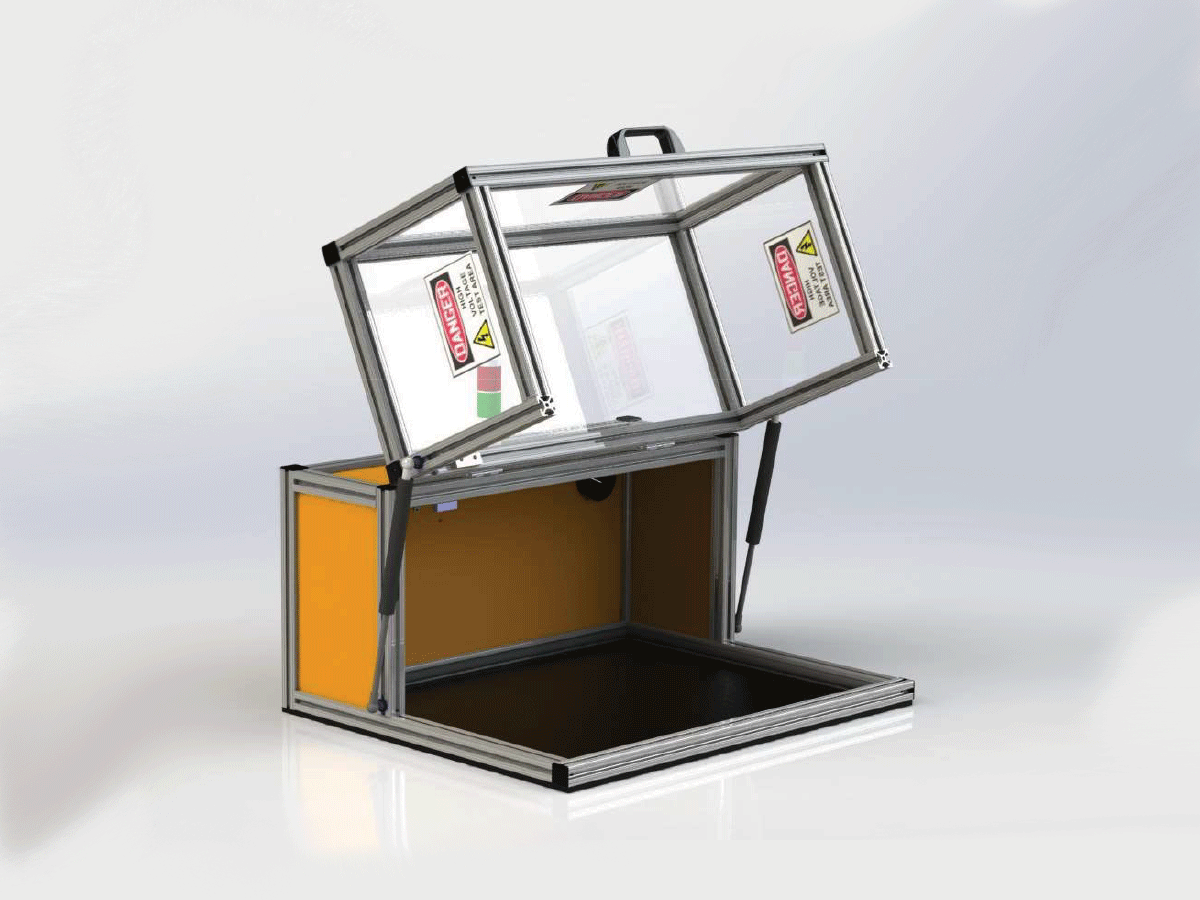
Press Release: Vitrek Announces New SE Series High Voltage Safety Enclosures
Vitrek Announces the SE Series of High Voltage Safety Enclosures The SE Series offers the utmost in operator safety for high voltage testing with solid aluminum frame construction, a durable acrylic cover and a magnetic interlock safety switch. […]