 Skip to content
Blogs
Semiconductor Wafer Lapping and Displacement Measurement
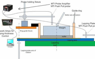
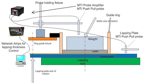
Semiconductor Wafer Lapping and Displacement Measurement Semiconductor Semiconductor Wafer Manufacturing Displacement Description Semiconductor Wafer Lapping and Displacement Measurement This application note explains how MTI's Accumeasure technology was used with a lapping machine to measure displacement (wafer material removal) and determine the new semiconductor wafer thickness. Changes in electrical capacitance (displacement) were measured and then directly converted into a 24-bit digital reading to obtain precise digital thickness measurements. During lapping, a wafer of known start thickness is placed on a rotary lapping table. The backside of the wafer faces downward and [...]
Measuring Piezoelectric Properties with Fiber Optics
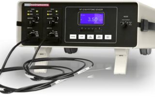
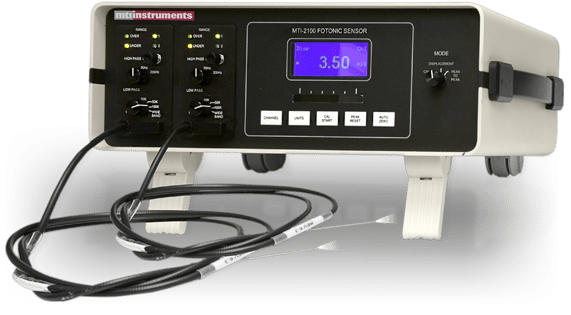
Measuring Piezoelectric Properties with Fiber Optics Research & Development Piezoceramic, 1-3 Pzt / Polymer Composite And Pvdf Film Amplitude Description Figure 4: Fiber Optic MTI 2100 Fotonic Sensor Introduction Researchers from the University of Arizona used the MTI-2000 Fotonic Sensor to measure the indirect piezoelectric properties (d33) and strain of bulk ferroelectric and thin film samples. The team then correlated these results with data acquired from direct piezoelectric effect measurement. By comparing data sets, the researchers concluded that the MTI-2000 provides a useful optical technique for measuring the [...]
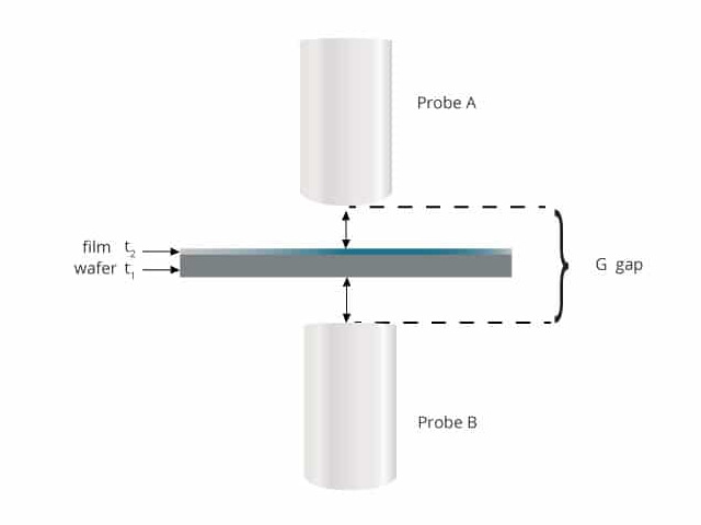
Thickness Gauge Measurement With Conductive Wafers and Thin Films
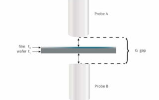
Thickness Gauge Measurement With Conductive Wafers and Thin Films Consumer Electronics Electronics Parts Profiling Thickness Description Using MTI's capacitive thickness gauge Proforma 300i with conductive wafers and thin films G = (a+b+t1+t2 ) Where G is the fixed gap between two probes When making the thickness measurement t2 can appear as t2 (film thickness) when it is a conductor, or 0 thickness when t2 is just air. So t2 will vary between the actual film thickness t2 if it's a conductor all the way down to 0 thickness if [...]
Two Ways to Measure Stamped Sheet Metal Thickness
Two Ways to Measure Stamped Sheet Metal Thickness Solar, Semiconductor Measurement of Ungrounded Targets Thickness, Metrology Description Learn how to measure stamped sheet metal thickness with MTI's Digital Accumeasure, a high-precision capacitance measurement system with nanometer accuracy and stability. Problem High silicon steels are alloys of iron and silicon that are easily magnetized and demagnetized. They can be supplied as sheet metal with a very thin dielectric coating. As this application note explains, precise measurements of stamped samples with a dielectric coating of ~ 10µi were needed. Solution MTI’s Digital [...]
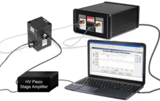
PIEZO STAGE POSITIONING
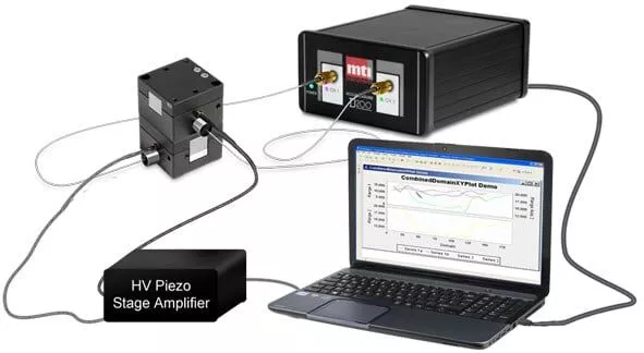
Industry Consumer Electronics Applications Piezo Stage Measurement Type Positioning Description Positioning stages using piezoelectric stack actuators (PEA) have very high resolution. However, it is difficult to achieve precise dynamic motion tracking using traditional linear controllers such as PID due to the inherent hysteresis nonlinearity of piezoelectric materials and the phase lag associated with such controllers. Capacitance Sensors are ideal for measuring the actual piezo stage position and correcting for the inherent nonlinearity through closed loop feedback. They have the stability, bandwidth and high resolution needed to do the job. [...]
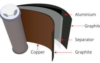
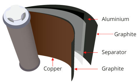
Two Ways to Measure EV Battery Plate Thickness
Two Ways to Measure EV Battery Plate Thickness Animation showing a system setup used to measure the thickness of thin conductive films such as electric vehicle (EV) battery electrodes. Description Learn how to measure EV battery plate thickness with MTI’s Digital Accumeasure, a high-precision capacitance measurement system with nanometer accuracy and stability. Problem Lithium battery plates for electric vehicles consist of lithium ion compounds applied to either a copper plate substrate (cathode plate) or an aluminum substrate (anode plate). The plates are approximately 100-200 um thick ( .004 - .008 inch). [...]
WAFER QA/QC AFTER SLICING AND POLISHING
Industry Semiconductor Applications Wafer Qa/Qc After Slicing And Polishing Measurement Type Surface Description When wafers are sliced up with wire saws, they are measured to make sure they are within the specified thickness, with minimal bow, warp, and TTV. After initial measurement, they are sorted and sent for polishing. Since polishing removes material and smoothes out the rough surfaces they need to be measured again to ensure they meet thickness guidelines and quality standards. Solution: MTI Instruments manufactures multiple systems to perform thickness measurements. From semi automated Proforma 300SA to manual wafer [...]
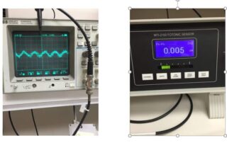
Dynamic Measurement of Small Oscillatory Motions
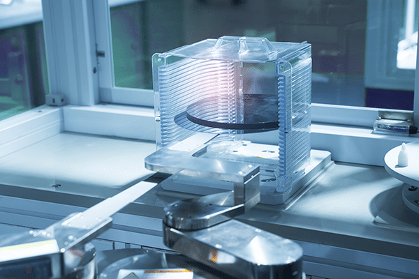
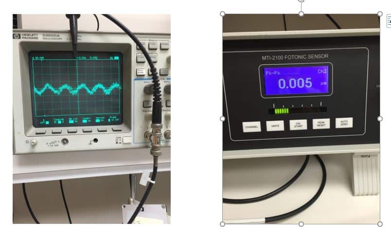
Dynamic Measurement of Small Oscillatory Motions Research & Development Piezoelectric Stack Motion Fotonic Systems Displacement Description This application note describes the measurement of a very small oscillatory motions (nanometers) produced by a piezo electric device with the MTI-2100 and the MTI-2032RX high-resolution module. Fotonic™ sensors from MTI Instruments are ideal for making dynamic measurements of very small oscillatory motions. Using the MTI-2100 Fotonic Sensor with a spectrum analyzer, angstrom level measurements are possible. Would you like to know more? Okay, let's set up some basic equipment and get started. Piezo [...]
ABOUT WAFER BOW AND WARP MEASUREMENT SYSTEMS
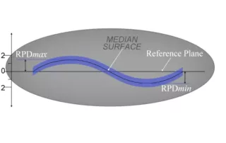
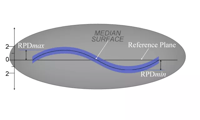
Thickness Measurement for Metrology Systems ASTM F657: The distance through a wafer between corresponding points on the front and back surface. Thickness is expressed in microns or mils (thousandths of an inch). Total Thickness Variation (TTV) ASTM F657: The difference between the maximum and minimum values of thickness encountered during a scan pattern or series of point measurements. TTV is expressed in microns or mils (thousandths of an inch). ASTM F534 3.1.2: The deviation of the center point of the median surface of a free, unclamped wafer from the median [...]
Interfacing MTI’s Digital Accumeasure to Measurement Computing’s DASYLab with Modbus
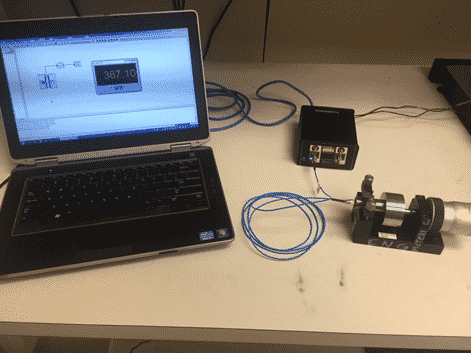
Interfacing MTI's Digital Accumeasure to Measurement Computing's DASYLab with Modbus Interfacing MTI's Digital Accumeasure to Measurement Computing's DASYLab with Modbus Displacement Description Laptop running MC DASYLab1 © and MTI Digital Capacitance sensor over Modbus TCP/IP Measurement Computing's DASYLab data acquisition software is easy to use and allows measuring with multiple system sensors (analog and digital). You can plot the results of multiple sensors versus time or encoder position and store the data with DASYLab. This application note describes how to interface MTI's Digital Capacitance Sensor over Ethernet TCP/IP. The DASYLab Modbus [...]