 Skip to content
Blogs
Digitizing Ultrasonic Signals
Digitizing Ultrasonic Signals Customer Case The customer has an ultrasonic signal that he wants to digitize with either 8 or 12-bit resolution. The sampling rate required for this application is a minimum of 16 MSPS (20 MSPS is acceptable). Finally, the data must be acquired for a full 10 seconds. The data is not coming in continuously: it is arriving in bursts one millisecond apart (PRF = 1 KHz). For each trigger the customer wants to capture approximately 200 us of data. Once this data is acquired, the customer wants it saved to the hard drive as a standard [...]
Digital Ultrasonic Array Data Capture
Digital Ultrasonic Array Data Capture Customer Case A customer possesses a commercial medical diagnostic ultrasonic system. The ultrasonic sensing head consists of an ultrasonic generator transducer and an 8' x 8' two-dimensional array of receiver transducers. The sensing head is pressed against the tissue under study and the generation transducer is periodically excited so that it emits a burst of ultrasonic energy. After each burst, the receiver array registers ultrasonic echoes reflected off tissue structures from each transducer element. In normal operation, digitized array data from each element is numerically processed and combined to construct a display image of [...]
 Using Capacitance Sensors for Non-Conductive Material Measurement Gallery
Using Capacitance Sensors for Non-Conductive Material Measurement
Application Notes-MTI, Brand-MTI, Industry-Compliance Testing, Industry-Consumer Products, Industry-Electronics, Industry-Manufacturing, Industry-Sensors, News-MTI, News-MTI-Instrumentation, Products-MTI-Capacitance, Z-REPUB, z1
Using Capacitance Sensors for Non-Conductive Material Measurement
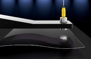
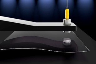
Non-Conductive Material Measurement with Capacitance Sensors Capacitance sensors are non-contact devices that can be used to obtain position, thickness, and dynamic measurements with a high degree of precision, accuracy, and resolution. Capacitive measurement is used with electrically-conductive materials such as metals but can also be used to measure non-conductive materials such as glass, sapphire, and many plastics. Even if a non-conductive material is relatively inexpensive (such as closed cell foam), manufacturers want to avoid errors that can result in significant waste across high volumes. Importantly, capacitance measurement is also used with semi-insulating materials such as gallium arsenide (GaAs) and [...]
Semiconductor Wafer Lapping and Displacement Measurement
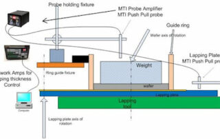
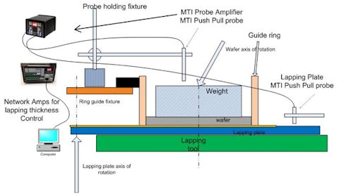
Semiconductor Wafer Lapping and Displacement Measurement Semiconductor Semiconductor Wafer Manufacturing Displacement Description Semiconductor Wafer Lapping and Displacement Measurement This application note explains how MTI’s Accumeasure technology was used with a lapping machine to measure displacement (wafer material removal) and determine the new semiconductor wafer thickness. Changes in electrical capacitance (displacement) were measured and then directly converted into a 24-bit digital reading to obtain precise digital thickness measurements. During lapping, a wafer of known start thickness is placed on a rotary lapping table. The backside of the wafer faces downward and [...]
Wafer Stress Analysis Using the 300iSA
Wafer Stress Analysis Using MTI Instruments Proforma 300iSAWafer processing involves several stages that may translate into mechanical alterations. Sometimes these alterations can cause deformities that render the wafer either unusable or that put it marginally close to not being usable. To determine this, stress analysis can be used.The Proforma 300iSA wafer characterization tool provides a software capability in which a wafer can be analyzed prior to processing and then after processing. The tool then evaluates how the wafer changed and hence, provides the resulting stress analysis.The software expects the customer to provide the material elasticity constants and to define them [...]
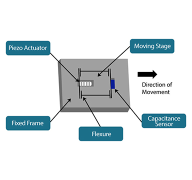
Capacitance Probes vs. Strain Gauges in Piezo Flexure Stages
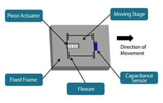
Capacitance probes with pico-positioning sensors can be embedded in piezo flexure stages. With minor mounting modifications, these non-contact probes provide significantly greater accuracy than strain gauges. Piezo flexure stages are positioning devices with a high degree of resolution. These motion stages contain a piezoelectric actuator that converts an electrical signal into displacement based on the reverse piezoelectric effect, which is the ability of a piezo electric material to elongate when a voltage is applied. When a voltage (e.g., 0-150 VDC) is applied to the actuator, the stage moves in proportion to the applied voltage. Yet, the exact position remains [...]
 CMP and Capacitance-Based Semiconductor Wafer Measurement Gallery
CMP and Capacitance-Based Semiconductor Wafer Measurement
Application Notes-MTI, Brand-MTI, Industry-Compliance Testing, Industry-Consumer Products, Industry-Electronics, Industry-Manufacturing, Industry-Semiconductor, Industry-Semiconductor-MTI, Industry-Sensors, Products-MTI-Capacitance, Products-MTI-Semiconductor/Metrology, z1
CMP and Capacitance-Based Semiconductor Wafer Measurement
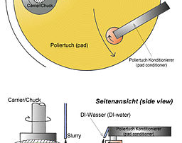
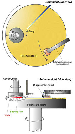
Chemical mechanical polishing (CMP) uses chemical oxidation and mechanical abrasion to selectively remove material from semiconductor wafers in order to achieve very high levels of planarity. The planarity, or flatness, of these wafers is important for optical lithography, a microfabrication technique that produces integrated circuits (ICs) by transferring a geometric pattern from a photomask to a light-sensitive chemical photoresist. Also known as photolithography or UV lithography, optical lithography can produce a geometric pattern on a thin film or directly onto the substrate. Semiconductor Wafer Measurements: Flatness and Shape During optical lithography, variations in wafer flatness must be smaller than [...]
 MTI Instrument’s PBS ROI Calculator: See How Much Money You Can Save Gallery
MTI Instrument’s PBS ROI Calculator: See How Much Money You Can Save
Application Notes-MTI, Brand-MTI, Industry-Aerospace, Industry-Compliance Testing, Industry-Government/Military, Industry-Manufacturing, Industry: Transportation, News-MTI, News-MTI-PBS, News-Products, Press Releases-Vitrek, Products-MTI, Products-MTI-Engine Balancing, Z-REPUB, z1
MTI Instrument’s PBS ROI Calculator: See How Much Money You Can Save
Ensuring the proper operation of your aircraft engine is essential to complying with manufacturers guidelines for the safety and longevity of the aircraft. Ensuring engines are not operating outside acceptible vibration limits and operating optimally isn't just smart, it is vital to your business. Excessive engine vibration can lead to cracked turbine, fan and compressor components potentially leading to catastrophic failure. The costs of catastrophic engine failure due to an unbalanced engine can measure in the millions of dollars. As airlines push to get more and more life out of their aging fleets, the need to properly maintain the [...]
 MEMS and Capacitance-Based Semiconductor Wafer Measurement Gallery
MEMS and Capacitance-Based Semiconductor Wafer Measurement
Application Notes-MTI, Brand-MTI, Industry-Compliance Testing, Industry-Consumer Products, Industry-Electronics, Industry-Manufacturing, Industry-Semiconductor, Industry-Semiconductor-MTI, Industry-Sensors, Products-MTI-Capacitance, Products-MTI-Semiconductor/Metrology, Z-REPUB, z1
MEMS and Capacitance-Based Semiconductor Wafer Measurement
MEMS Technology and Capacitance-Based Wafer Measurement Micro-electrical-mechanical systems (MEMS) are tiny devices that house electrical and mechanical components on a single silicon chip or integrated circuit (IC). They integrate mechanical structures with electronics that are normally fabricated with complementary metal-oxide-semiconductor (CMOS) technologies. In addition to miniaturization, the benefits of MEMS include expanded functionalities at lower cost and with improved performance and reliability. With MEMS devices, critical physical dimensions range from smaller than one micron (µ) to larger than several millimeters (mm). In complex systems, multiple moving elements may be controlled by integrated electronics. Examples of the mechanical components in [...]
PAxx Power Analyzers using External Current Sensors: Application Notes
Current Sensors use two main techniques. A current transformer divides current. So for instance a 100:1 current transformer would see an input of 10A and output 100mA. Note that this technique is only useful for AC current. When using a current transformer you can directly input the current into one of our internal shunts as long as you stay within the current limitations of the input. Notice that current transformers are inductive so they act as a low pass filter. If you use a current transformer it is important to select a transformer that will work accurately at your frequency [...]