 Skip to content
Blogs
Semiconductor Wafer Lapping and Displacement Measurement
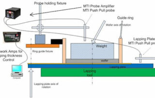
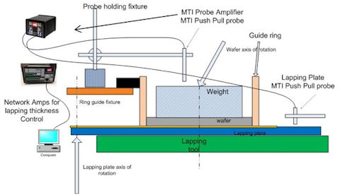
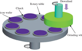
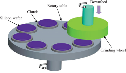
Semiconductor Wafer Lapping and Displacement Measurement Semiconductor Semiconductor Wafer Manufacturing Displacement Description Semiconductor Wafer Lapping and Displacement Measurement This application note explains how MTI’s Accumeasure technology was used with a lapping machine to measure displacement (wafer material removal) and determine the new semiconductor wafer thickness. Changes in electrical capacitance (displacement) were measured and then directly converted into a 24-bit digital reading to obtain precise digital thickness measurements. During lapping, a wafer of known start thickness is placed on a rotary lapping table. The backside of the wafer faces downward and [...]
Wafer Stress Analysis Using the 300iSA
Wafer Stress Analysis Using MTI Instruments Proforma 300iSAWafer processing involves several stages that may translate into mechanical alterations. Sometimes these alterations can cause deformities that render the wafer either unusable or that put it marginally close to not being usable. To determine this, stress analysis can be used.The Proforma 300iSA wafer characterization tool provides a software capability in which a wafer can be analyzed prior to processing and then after processing. The tool then evaluates how the wafer changed and hence, provides the resulting stress analysis.The software expects the customer to provide the material elasticity constants and to define them [...]
Capacitance Probes vs. Strain Gauges in Piezo Flexure Stages
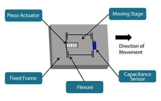
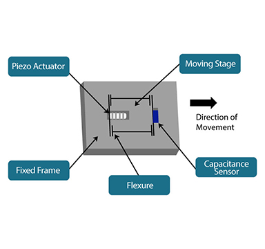
Capacitance probes with pico-positioning sensors can be embedded in piezo flexure stages. With minor mounting modifications, these non-contact probes provide significantly greater accuracy than strain gauges. Piezo flexure stages are positioning devices with a high degree of resolution. These motion stages contain a piezoelectric actuator that converts an electrical signal into displacement based on the reverse piezoelectric effect, which is the ability of a piezo electric material to elongate when a voltage is applied. When a voltage (e.g., 0-150 VDC) is applied to the actuator, the stage moves in proportion to the applied voltage. Yet, the exact position remains [...]
 CMP and Capacitance-Based Semiconductor Wafer Measurement Gallery
CMP and Capacitance-Based Semiconductor Wafer Measurement
Application Notes-MTI, Brand-MTI, Industry-Compliance Testing, Industry-Consumer Products, Industry-Electronics, Industry-Manufacturing, Industry-Semiconductor, Industry-Semiconductor-MTI, Industry-Sensors, Products-MTI-Capacitance, Products-MTI-Semiconductor/Metrology, z1
CMP and Capacitance-Based Semiconductor Wafer Measurement
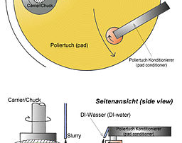
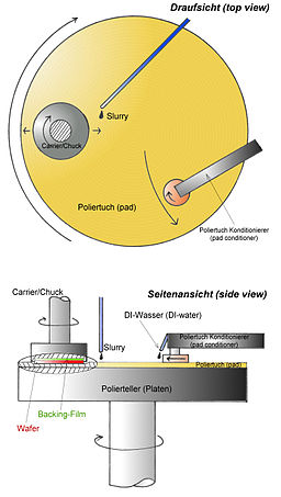
Chemical mechanical polishing (CMP) uses chemical oxidation and mechanical abrasion to selectively remove material from semiconductor wafers in order to achieve very high levels of planarity. The planarity, or flatness, of these wafers is important for optical lithography, a microfabrication technique that produces integrated circuits (ICs) by transferring a geometric pattern from a photomask to a light-sensitive chemical photoresist. Also known as photolithography or UV lithography, optical lithography can produce a geometric pattern on a thin film or directly onto the substrate. Semiconductor Wafer Measurements: Flatness and Shape During optical lithography, variations in wafer flatness must be smaller than [...]
 MTI Instrument’s PBS ROI Calculator: See How Much Money You Can Save Gallery
MTI Instrument’s PBS ROI Calculator: See How Much Money You Can Save
Application Notes-MTI, Brand-MTI, Industry-Aerospace, Industry-Compliance Testing, Industry-Government/Military, Industry-Manufacturing, Industry: Transportation, News-MTI, News-MTI-PBS, News-Products, Press Releases-Vitrek, Products-MTI, Products-MTI-Engine Balancing, Z-REPUB, z1
MTI Instrument’s PBS ROI Calculator: See How Much Money You Can Save
Ensuring the proper operation of your aircraft engine is essential to complying with manufacturers guidelines for the safety and longevity of the aircraft. Ensuring engines are not operating outside acceptible vibration limits and operating optimally isn't just smart, it is vital to your business. Excessive engine vibration can lead to cracked turbine, fan and compressor components potentially leading to catastrophic failure. The costs of catastrophic engine failure due to an unbalanced engine can measure in the millions of dollars. As airlines push to get more and more life out of their aging fleets, the need to properly maintain the [...]
 MEMS and Capacitance-Based Semiconductor Wafer Measurement Gallery
MEMS and Capacitance-Based Semiconductor Wafer Measurement
Application Notes-MTI, Brand-MTI, Industry-Compliance Testing, Industry-Consumer Products, Industry-Electronics, Industry-Manufacturing, Industry-Semiconductor, Industry-Semiconductor-MTI, Industry-Sensors, Products-MTI-Capacitance, Products-MTI-Semiconductor/Metrology, Z-REPUB, z1
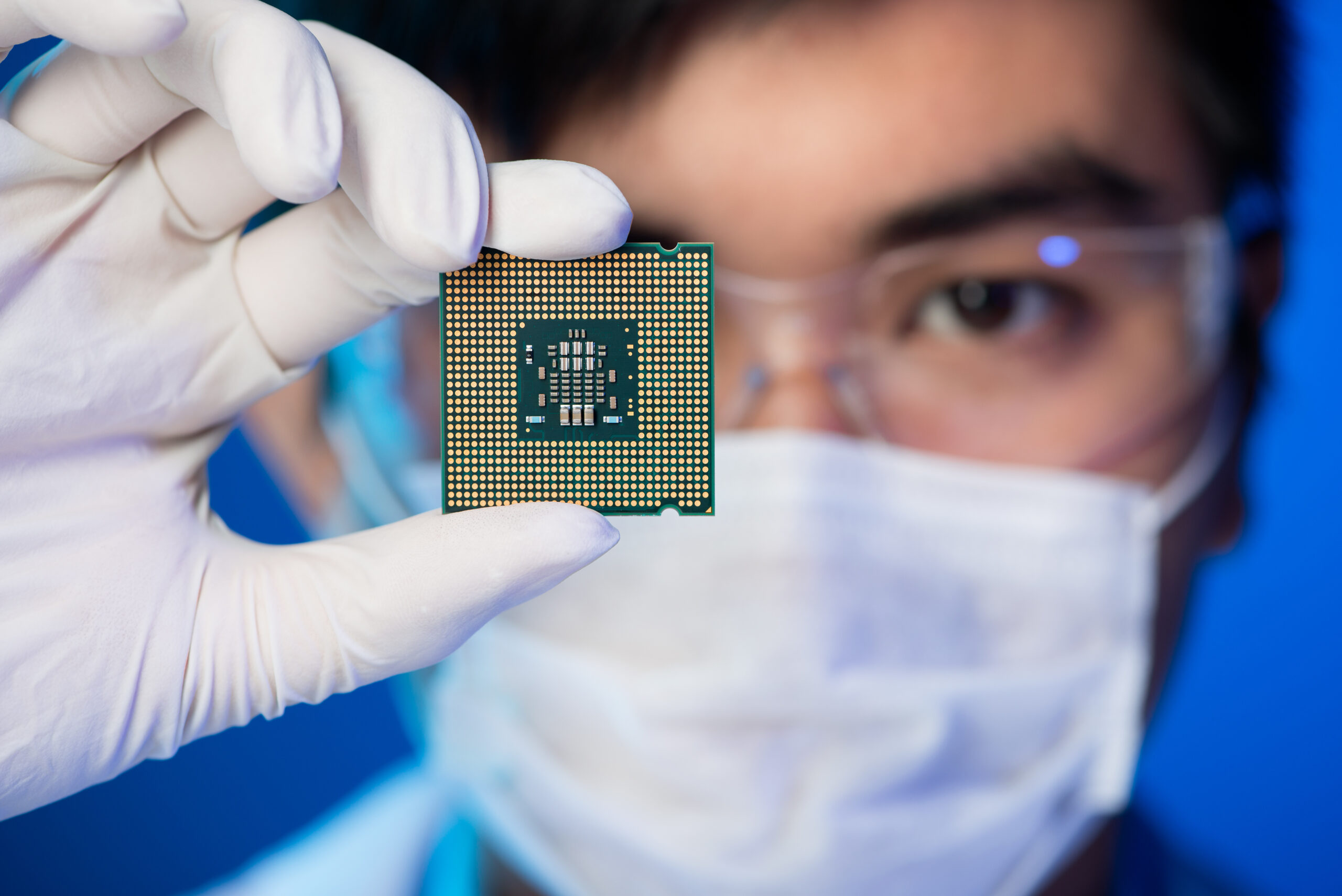
MEMS and Capacitance-Based Semiconductor Wafer Measurement
MEMS Technology and Capacitance-Based Wafer Measurement Micro-electrical-mechanical systems (MEMS) are tiny devices that house electrical and mechanical components on a single silicon chip or integrated circuit (IC). They integrate mechanical structures with electronics that are normally fabricated with complementary metal-oxide-semiconductor (CMOS) technologies. In addition to miniaturization, the benefits of MEMS include expanded functionalities at lower cost and with improved performance and reliability. With MEMS devices, critical physical dimensions range from smaller than one micron (µ) to larger than several millimeters (mm). In complex systems, multiple moving elements may be controlled by integrated electronics. Examples of the mechanical components in [...]
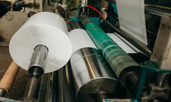
Measuring the Step Height Thickness of Non- Woven Conductive Films
Establishing and maintaining product quality throughout the production process is a common challenge of all manufacturers. How does an organization ensure the optimal output from their production lines, especially in real time? Key to this is strong non-destructive measurement practices that can take place at various points along the production process. The case study below is an example of how this was done at Saint-Gobain to measure the thickness and density of foam materials. They engaged with MTI's team of experts as their current direction was proving cost-prohibitive. Saint-Gobain's R&D organization, led by Dr. Mickael Boinet, found a solution [...]
Improving Performance of Gas Compressors
Improving Performance of Gas Compressors Customer Case A customer who is a manufacturer of natural gas compressors is seeking to improve the efficiency of their 12-cylinder diesel engines. These diesel engines are used to drive the gas compressors. The performance of the engines is analyzed from the position of the engines' shaft, which is detected by an optical encoder. The output from the encoder is a 12 kHz jittery clock with variable pulse width. The jitter has high frequency components and the jitter variation can go down to 0.1 microsecond and varies systematically with wear, load, fuel and other [...]
 Wafer Backgrinding and Semiconductor Thickness Measurements Gallery
Wafer Backgrinding and Semiconductor Thickness Measurements
Application Notes-MTI, Brand-MTI, Industry-Compliance Testing, Industry-Consumer Products, Industry-Electronics, Industry-Manufacturing, Industry-Semiconductor, Industry-Semiconductor-MTI, News-MTI-Instrumentation, News-MTI-Metrology, Products-MTI-Capacitance, Products-MTI-Semiconductor/Metrology, Z-REPUB, z1
Wafer Backgrinding and Semiconductor Thickness Measurements
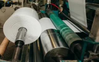
Wafer backgrinding is the first step in semiconductor packaging, the process of encasing one or more discrete semiconductor devices or integrated circuits (IC) for protection. Known also as wafer thinning or wafer lapping, backgrinding reduces wafer thickness to allow stacking and high-density IC packaging. Wafer thickness also determines package height, an important consideration as smartphones, laptops, and other electronic devices become thinner. With MEMS, wafer thinning also controls the proof mass for devices such as accelerometers or the diaphragm thickness for pressure sensors. Etching the surface of the wafer produces the IC but grinding the backside is what produces [...]
 Silicon Carbide vs. Silicon in EV Power Electronics Gallery
Silicon Carbide vs. Silicon in EV Power Electronics
Application Notes-MTI, Brand-MTI, Industry-Automotive, Industry-Battery, Industry-Compliance Testing, Industry-Consumer Products, Industry-Electronics, Industry-Government/Military, Industry-Manufacturing, Industry-R&D, News-MTI-Instrumentation, Products-MTI-Capacitance, Z-REPUB, z1
Silicon Carbide vs. Silicon in EV Power Electronics
Compare silicon carbide vs. silicon for electric vehicle (EV) power electronics and learn about SiC wafer measurement. As demand for electric vehicles (EVs) continues to grow, manufacturers are comparing two semiconductor technologies, silicon carbide and silicon, for power electronics applications. Silicon carbide (SiC) provides the high temperature resistance, low power consumption, rigidity, and support for smaller, thinner designs that EV power electronics need. Examples of SiC’s current applications include on-board DC/DC converters, off-board DC fast chargers, on-board battery chargers, EV powertrains, and automotive lighting for LEDs. According to Automotive World, SiC technology could also drive future EV innovations [...]