 Skip to content
Blogs
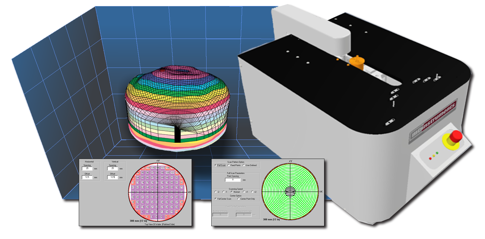
 The Benefits of Manual, Semi-Automated, and Fully-Automated Systems for Semiconductor Wafer Inspection and Metrology Gallery
The Benefits of Manual, Semi-Automated, and Fully-Automated Systems for Semiconductor Wafer Inspection and Metrology
Application Notes-MTI, Brand-MTI, Industry-Consumer Products, Industry-Electronics, Industry-Manufacturing, Industry-Semiconductor, Industry-Semiconductor-MTI, News-MTI-Metrology, Products-MTI-Semiconductor/Metrology, z1
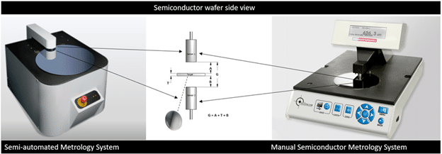
The Benefits of Manual, Semi-Automated, and Fully-Automated Systems for Semiconductor Wafer Inspection and Metrology
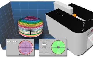
This is the third of three articles in Semiconductor Wafer Measurement for Increased Profitability. The first article in this series explains why disc geometry matters. The second article examines the cost of failing to inspect semiconductor wafers. Fully automated systems that can load, scan, and unload wafers are fast, convenient, and efficient at high volumes. They’re useful for checking every wafer in every batch, but these systems are expensive. Semi-automated and manual systems cost significantly less and are generally used for lower volumes; however, they’re also easy-to-use and can make fast, accurate measurements that support production flow. Semi-automated and [...]
 Why Disc Geometry Matters In Wafer Production Gallery
Why Disc Geometry Matters In Wafer Production
Application Notes-MTI, Brand-MTI, Industry-Consumer Products, Industry-Electronics, Industry-Manufacturing, Industry-Semiconductor, Industry-Semiconductor-MTI, News-MTI-Metrology, Products-MTI-Semiconductor/Metrology, z1
Why Disc Geometry Matters In Wafer Production
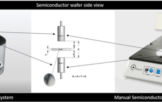
This is the first of three articles in Semiconductor Wafer Measurement for Increased Profitability. The second article examines the cost of failing to inspect semiconductor wafers. The third article describes the benefits of using semi-automated, fully-automated, and manual systems for wafer metrology and inspection. Semiconductor wafers are cut from cylindrical silicon crystals, or ingots. The flatness of these disc-shaped wafers is controlled to tight tolerances to ensure that the entire wafer surface is suitable for integrated circuit (IC) production. If disc geometry is out-of-spec after cutting, it may be possible to reprocess the wafer. Cutting is only the first [...]

How Capacitive Measurement Can Help Reduce Packaging Waste
Product packaging is often made of lightweight polymeric foams or plastic sheets and films. These materials are relatively inexpensive, but manufacturers still want to minimize waste and maximize yields. Across high volumes of low-cost materials, even a small per-unit savings can become significant, especially as the price of petroleum – a key ingredient in many polymers – continues to rise. For companies with environmental sustainability efforts, there are other important considerations as well. The excessive use of packaging materials can contribute to environmental pollution, especially with polymers that are slow to degrade. Yet, materials such as plastic sheets and [...]
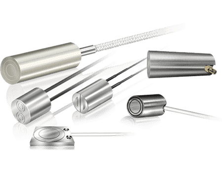
Non-Contact Displacement Sensors for Detection and Measurement
Non-contact sensors detect or measure a physical property without making direct contact with the target, the object that is being monitored or measured. They are used to measure physical properties such as thickness, proximity, displacement, or distance. To obtain readings, non-contact displacement sensors emit a form of energy and may use capacitance, fiber optic, or laser triangulation technologies. By contrast, contact sensors must touch the target and often rely upon mechanical movement. Non-Contact Sensors vs. Contact Sensors Non-contact sensors are faster, especially for applications with high sampling rates, and won’t dampen the motion of a target. They can also [...]
 Advantages of Measuring Semiconductor Thin Film Thickness with Capacitance Gallery
Advantages of Measuring Semiconductor Thin Film Thickness with Capacitance
Application Notes-MTI, Brand-MTI, Industry-Compliance Testing, Industry-Electronics, Industry-Manufacturing, Industry-R&D, Industry-Semiconductor, Industry-Semiconductor-MTI, Industry-Sensors, Products-MTI-Capacitance, Products-MTI-Laser/Fiber Optic, Products-MTI-Semiconductor/Metrology, Z-REPUB, z1
Advantages of Measuring Semiconductor Thin Film Thickness with Capacitance
Semiconductor Thin Films: Measuring Thickness with Capacitance In the semiconductor industry, thin films are deposited onto silicon and other wafer materials one atomic layer at a time. The thickness of these extremely thin coatings is important because thin-film thickness affects the wafer’s electrical, optical, and mechanical properties. With semiconductors, either conductive metallic films or non-conductive metal oxide films are deposited. There are two main thin-film coating methods, chemical vapor deposition (CVD) and physical vapor deposition (PVD), both of which use a variety of processes. Because the coatings for semiconductor wafers are so thin, thickness measurement require a high degree [...]
CEMENT BOARD QUALITY CONTROL
Cement backer board is used as underlayment for tile floors, walls and counter tops. It is also used as exterior sheathing and in exterior stucco systems. Cement backer board has proven to be more durable than virtually any other underlayment if quality control and thickness is maintained. The Problem: A major cement board manufacturer was faced with the challenge to improve a board production line throughput and decrease the amount of waste in the process. Too thin of cement board material weakens it structurally, while board that is too thick wastes material and resources, as well as drives up production costs. [...]
How Often Should Vibration Analysis Be Performed?
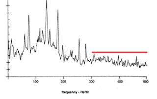
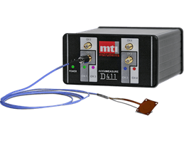
How Often Should Vibration Analysis Be Performed? Once a customer takes delivery of a PBS system and learns how to use it, the next logical question is: “How often should we use it?” At a minimum, your approved maintenance program (whether it’s a program developed by your operation, or the maintenance procedures outlined by the engine/airframe manufacturer) will tell you about the intervals at which to perform a vibration analysis. Usually, there is a procedure to specify how an engine vibration analysis and balance need be only completed when squawked by a pilot or after the completion of maintenance work [...]
 Contact vs. Non-Contact Measurement and Linear Displacement Sensors Gallery
Contact vs. Non-Contact Measurement and Linear Displacement Sensors
Application Notes-MTI, Brand-MTI, Industry-Compliance Testing, Industry-Consumer Products, Industry-Electronics, Industry-Manufacturing, Industry-Semiconductor, Industry-Semiconductor-MTI, Industry-Sensors, Products-MTI-Capacitance, Z-REPUB, z1, ZOK
Contact vs. Non-Contact Measurement and Linear Displacement Sensors
Contact vs. Non-Contact Measurement and Linear Displacement Sensors Linear displacement sensors are used to measure the distance between two points or two plane surfaces. They use various technologies, but there are two basic types: contact and non-contact. As their names suggest, contact sensors make physical contact with the object that is being measured and non-contact sensors do not. This is an obvious but important difference, but there is much more to consider. Non-contact measurement is faster than contact measurement, especially for applications with high sampling rates. Because contact-type devices must touch and then traverse the object, measurement is slower. [...]
Capacitance Sensors vs. Eddy Current Sensors Application Note
Capacitance Sensors vs. Eddy Current Sensors Application Note Capacitance sensors and Eddy current sensors are both used for non-contact measurements. Capacitive probes use electric fields to measure the distance from the sensor face to the surface of a target that is typically conductive and grounded. Eddy current probes use an alternating AC current to induce a magnetic field in a conductive target instead. In turn, the induced magnetic field produces a back magnetic field that is proportional to the gap between the probe face and the target. In a recent application note, MTI Instruments examines the differences between capacitance [...]
 Using Capacitance Sensors for Non-Conductive Material Measurement Gallery
Using Capacitance Sensors for Non-Conductive Material Measurement
Application Notes-MTI, Brand-MTI, Industry-Compliance Testing, Industry-Consumer Products, Industry-Electronics, Industry-Manufacturing, Industry-Sensors, News-MTI, News-MTI-Instrumentation, Products-MTI-Capacitance, Z-REPUB, z1
Using Capacitance Sensors for Non-Conductive Material Measurement
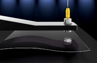
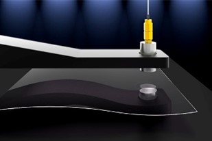
Non-Conductive Material Measurement with Capacitance Sensors Capacitance sensors are non-contact devices that can be used to obtain position, thickness, and dynamic measurements with a high degree of precision, accuracy, and resolution. Capacitive measurement is used with electrically-conductive materials such as metals but can also be used to measure non-conductive materials such as glass, sapphire, and many plastics. Even if a non-conductive material is relatively inexpensive (such as closed cell foam), manufacturers want to avoid errors that can result in significant waste across high volumes. Importantly, capacitance measurement is also used with semi-insulating materials such as gallium arsenide (GaAs) and [...]