Blogs
Hopkinson Bar Testing (Stress Pulse Reaction Testing)
Hopkinson Bar Testing (Stress Pulse Reaction Testing) Customer Case This customer is involved in testing materials for how they react to stress pulses. The idea is to introduce a stress pulse into the Material Under Test (MUT) and monitor it as it travels through the material. This method of material characterization is also known as "Hopkinson Bar" testing. Multiple sensors pick up the reaction of the material and provide outputs which need to be digitized. These outputs are transient signals of approximately 2 Volts and have a rise time of approximately 600 nanoseconds. The resulting system must be programmable [...]
 Transducer Selection for High Resolution Applications Gallery
Transducer Selection for High Resolution Applications
Application Notes-MTI, Brand-MTI, News-MTI-Instrumentation, News-MTI-Metrology, News-Product Updates, News-Products, Products-MTI-Capacitance, Products-MTI-Laser/Fiber Optic, Products-MTI-Semiconductor/Metrology, Products-MTI-Signal Generators, Z-REPUB, z1
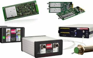
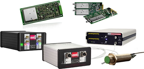
Transducer Selection for High Resolution Applications
High resolution applications do not always require an interferometer. If you want to make accurate measurements in the micron to picometer range, then an MTI Digital Accumeasure D100 HD or D200 system may be what you need. Laser interferometers can sell for more than $15,000 and be difficult to setup. For example, you may have to buy additional optics to guarantee a good return signal since the laser beam must reflect off a mirror surface or precision retro reflector in order for the beam to re-enter the interferometer’s optics at less than a degree of reflection angle. The downsides [...]
Vibration Test Equipment Instrument Grade Chassis
Vibration Test Equipment Instrument Grade Chassis Customer Case The customer is in the business of building Vibration Test equipment for semiconductor, automotive and aerospace industries. Their product is currently housed in Industrial Grade PCs which they integrate themselves. They currently purchase the chassis from an off-shore company. Their major problem is product differentiation: their product looks like "just another PC" and, therefore, cannot command a better price point. They also presently have to ship a separate monitor, as one is not integrated in the chassis. They want to upgrade the chassis to one of better quality, with a more [...]
Non-Destructive Testing (NDT)
Non-Destructive Testing (NDT) Customer Case This customer manufactures non-destructive test equipment which allows customers such as steel mills to test the quality of their end-products. Presently, the ultrasound frequencies being used are centered at either 5 MHz, 10 MHz or 15 MHz. The worst case analog bandwidth requirement in this case is 35 MHz. In order to set up their equipment properly, the customer presently views the return signal (including the flaw) on an analog oscilloscope with a sweep time of either 50 us or 100 us (providing approximately 5 to 10 inches of depth in a metal). The [...]
Check Out Vitrek’s Available Education and Product Training Resources
At Vitrek, we do more than just design and build high-quality electrical testing equipment — we ensure that our customers have all of the tools that they need to succeed when using our products. Here, we offer an overview of the plethora of educational resources that we have available on our website. […]
Acoustic Micro-Imaging
Acoustic Micro-Imaging Customer Case The customer is a leader in the field of acoustic micro-imaging. They use pulse ultrasound to image non-human materials. The ultrasound frequency used is between 100 and 200 MHz, as the materials they study can handle these frequencies (one cannot normally use such high frequencies with human tissue). The customer's PRF (Pulse Repeat Frequency) is approximately 4 KHz, with a PRI (Pulse Repeat Interval) of 250 ms. They need to capture approximately 2 ms (1,000 points) of data for each pulse. The customer wants scope emulation software to allow verification of board operation without having [...]
 High Resolution Semiconductor Wafer Measurements at Lower Costs Gallery
High Resolution Semiconductor Wafer Measurements at Lower Costs
Application Notes-MTI, Brand-MTI, Industry-Consumer Products, Industry-Electronics, Industry-Manufacturing, Industry-Semiconductor, Industry-Semiconductor-MTI, Products-MTI-Capacitance, Products-MTI-Semiconductor/Metrology, Z-REPUB, z1
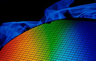
High Resolution Semiconductor Wafer Measurements at Lower Costs
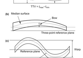
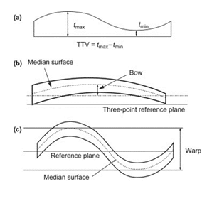
MTI's Proforma technology characterizes semiconductor wafers in terms of bow and warp, thickness, total thickness variation (TTV) and center thickness. Until recently, semiconductor wafer measurements at resolutions less than 100 µm were cost-prohibitive. Moreover, only expensive devices such as interferometers were capable of these measurements. Today, the semiconductor industry can use capacitance gauges instead of laser interferometers to achieve high resolution at fraction of the cost. Much like affordable CCD cameras transformed and expanded the market for video, cost-effective capacitance is disrupting the semiconductor wafer measurement market and creating new opportunities for quality testing and validation. The [...]
Non-Destructive Testing (NDT) Scanning Inspection
Non-Destructive Testing (NDT) Scanning Inspection Customer Case The customer is testing interior of pipes with time-resolved fluorescence, a Photo Multiplier Tube (PMT), a transducer with 8 MHz BandWidth and an integration chamber. They are searching for rare events and the scan width is approximately 3.5 inches. Multiple Record: 350 scans x 3 Kpts. GaGe Case Solution We recommended 5X-10X over sampling - therefore CompuScope 14100, CompuScope 12100, or even the 8-bit CS8500 may be sufficient. For a CS8500 Single Record example, say, at the single-channel sampling-rate of 50 MS/s, a 3000 point (i.e. 3 KS) acquisition would take about [...]
 Measure Wafer Bow, Warp and TTV with Capacitance Gallery
Measure Wafer Bow, Warp and TTV with Capacitance
Application Notes-MTI, Brand-MTI, Industry-Battery, Industry-Compliance Testing, Industry-Consumer Products, Industry-Electronics, Industry-Manufacturing, Industry-Semiconductor, Industry-Semiconductor-MTI, Industry-Sensors, Products-MTI-Capacitance, Z-REPUB, z1, ZOK
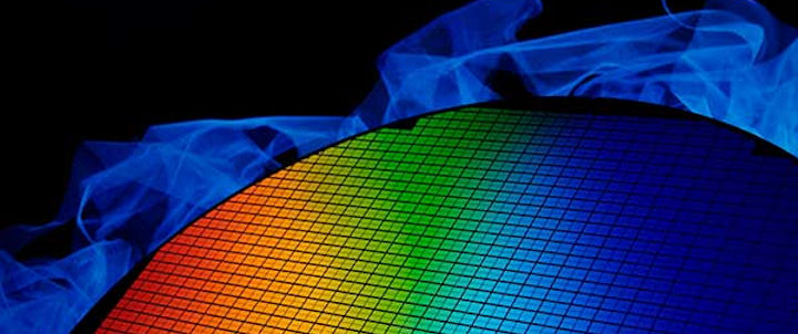
Measure Wafer Bow, Warp and TTV with Capacitance
The flatness of silicon wafers used to manufacture integrated circuits is controlled to tight tolerances to help ensure that the whole wafer is sufficiently flat for lithographic processing. To ensure your wafer manufacturing process is within tolerance, you need to measure the wafers being produced. Various measurement techniques exist to verify process tolerances and eliminate expensive scrap wafers. Non-contact capacitive sensing is a highly precise and cost-effective means to measure wafer flatness, bow, warp, and total thickness variation (TTV). MTI Instruments’ Proforma 300i and 300iSA systems use capacitance sensors to improve yields while reducing costs through better dimensional control of [...]