 Skip to content
Blogs
Wire Bonding
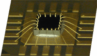
Wire Bonding Semiconductor Wire Bonding Level Description Introduction:  Machine automation frequently involves measuring small distances extremely accurately. Wire Bonding is one such application with some challenging requirements. A ‘normal’ wire bond consists of gold wire bonded to a substrate (PC Board) and an integrated circuit. Wire size varies between eighteen and fifty microns, with twenty-five microns being the ‘standard’; pad sizes are typically between seventy-five and one hundred microns wide. Space between two pads is generally one hundred microns. The width of the actual bond is generally 1.2 to 2.5 times [...]
GaAs Substrate Thickness Measurement
GaAs Substrate Thickness Measurement Semiconductor Gaas Substrate Thickness Measurement Thickness Description Measuring Thickness of Wafers with Different Chemistries Introduction:  Silicon wafers are ordinarily highly conductive and easy to measure with standard capacitive displacement sensors (See MTI's Proforma 300i). Measuring the thickness of GaAs wafers that have high bulk resistivity (>10k Ohm/cm) is a little more difficult because the wafers act as non-conductive insulators in a capacitive sensor's measuring field. Fortunately, MTI has a solution to this problem. Solution:  It’s possible to measure the thickness and TTV of high resistivity semiconducting [...]

Hard Drive Position
Semiconductor Hard Drive Position Positioning Description

LED Substrate Thickness
LED Substrate Thickness Semiconductor Led Substrate Thickness Thickness Description Remember that old acronym, GIGO?  Garbage in garbage out, it can apply to raw materials as well as programming. Sapphire wafers need to be of a certain quality to ensure maximum yield. Excessive TTV, Bow, and Warp lead to premature LED failure. LED manufacturers need to inspect incoming wafers. Wafer producers also need to check and control TTV, Bow and Warp. The market for sapphire wafers, driven by the growth in LED manufacturing, is booming. While the price has come down [...]

Photolithography Using Capacitance Sensors
Photolithography Using Capacitance Sensors Semiconductor Photolithography Using Capacitance Sensors Positioning Description When it comes to photolithography, how accurate are our sensors? Accurate enough to measure this: ​   Photo by D. Carr and H. Craighead, Cornell The world's smallest guitar is 10 micrometers long -- about the size of a single cell -- with six strings each about 50 nanometers, or 100 atoms, wide. Made by Cornell University researchers from crystalline silicon, it demonstrates a new technology for a new generation of electromechanical devices. Even the world’s smallest guitar’s 2 [...]